Touch panel-integrated liquid crystal display device

a liquid crystal display device and touch panel technology, applied in the field of touch panel, can solve the problems of increasing the size of the periphery, increasing the total thickness, and requiring numerous manual mounting operations, so as to reduce the total number of substrates used and optimize the connection

Active Publication Date: 2011-06-16
LG DISPLAY CO LTD
View PDF8 Cites 134 Cited by
  • Summary
  • Abstract
  • Description
  • Claims
  • Application Information

AI Technical Summary

Benefits of technology

[0036]It is one object of the present invention to provide a touch panel-integrated liquid crystal display device wherein a touch panel is formed on an outer surface of a substrate in a liq

Problems solved by technology

Such mounting areas cause an increase in the size of the periphery.
Also, connectors should be separately provided, disadvantageously requiring numerous manual labor-intensive mounting operations.
In this case, a process for forming the touch panel 20, apart from the liquid crystal panel 10, and a process for adhering the touch panel 20 to the liquid crystal panel 10 are required, disadvantageously causing an increase in total thickness caused by use of a plurality of substrates and lengthened process period.
First, the touch panel and the liquid crystal panel are separately formed and an adhesive layer is interposed between the panels to join the panels. As a result, the total number of glass substrates required is four to five, that is, two substrates for the liquid crystal panel and two substrates for the touch panel and a cover glass, thus making it impossible to reduce the thickness of the liquid crystal display device. That is, for example, the glass substrate is the thickest, about 0.

Method used


Image

  • Touch panel-integrated liquid crystal display device
  • Touch panel-integrated liquid crystal display device
  • Touch panel-integrated liquid crystal display device

Examples


first embodiment

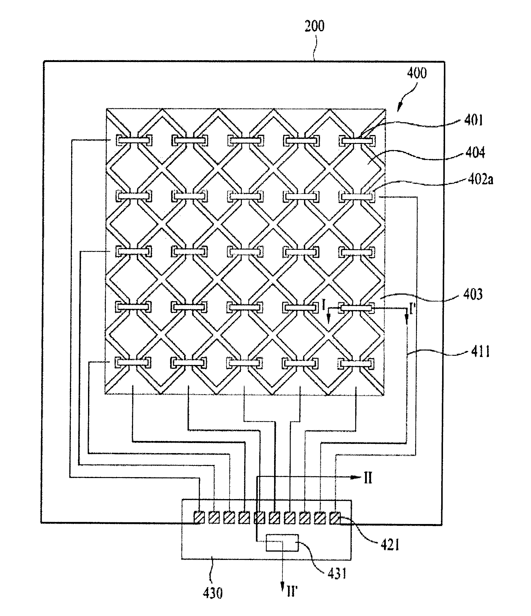
[0105]FIG. 5 is a plan view illustrating connection between a touch panel driving portion and a liquid crystal panel driving portion for a touch panel-integrated liquid crystal display device according to the present invention.

[0106]As shown in FIG. 5, for the touch panel-integrated liquid crystal display device according to the first embodiment, the FPC 430 for driving the touch panel 400 is formed at one outer surface (upper part of the drawing) of the second substrate 200 and the PCB 150 for driving the liquid crystal panel is formed at the other side (lower part of the drawing) of the first substrate 100.

[0107]In this case, the other side provided with the PCB 150 of the first substrate 100 protrudes, as compared to the second substrate 200, the seal pattern (reference numeral “250” in FIG. 4 of the first and second substrates 100 and 200 is formed at the edge in which the first and second substrates 100 and 200 overlap each other, partially overlaps the seal pattern 250 and the...

second embodiment

[0114]FIG. 6 is a plan view illustrating connection between a touch panel driving portion and a liquid crystal driving portion for a touch panel-integrated liquid crystal display device according to the present invention.

[0115]The touch panel-integrated liquid crystal display device according to the second embodiment shown in FIG. 6 is different from that of the first embodiment in that FPCs 430a and 430b are arranged at both sides of the second substrate 200.

[0116]Similarly, the FPCs 430a and 430b are formed in a different direction than the PCB 150, and the first substrate 100 overlaps the second substrate 200 at one side in which the FPCs 430a and 430b are formed. In this overlap region, there is no risk of shorting of metal lines formed in the FPCs 430a and 430b. Also, an additional double-sided tape is provided at one side of the first substrate 100 or second substrate 200 corresponding to the FPCs 430a and 430b to allow the FPCs 430a and 430b to be bent to a lower part of the ...

third embodiment

[0118]FIG. 7 is a plan view illustrating connection between a touch panel driving portion and a liquid crystal panel driving portion for a touch panel-integrated liquid crystal display device according to the present invention. FIG. 8 is a perspective view illustrating a variant of the touch panel-integrated liquid crystal display device of FIG. 7.

[0119]As shown in FIGS. 7 and 8, for the touch panel-integrated liquid crystal display device according to the third embodiment, FPCs 440a and 440b alternate with the COF 130 connected to the PCB 150 on the side at which the PCB 150 is formed. At this time, when one side of FPCs 440a and 440b is connected to the pad electrode of the touch panel in order to drive the touch panel and is bent at one side of the second substrate 200, the other side thereof is connected to the PCB 150. That is, in this case, the other side of the FPC 440a or 440b is connected to one side of the PCB 150 to synchronize and control operation of the touch panel thr...


PUM


Abstract

A liquid crystal display device includes a liquid crystal panel comprising a first substrate and a second substrate, a seal pattern arranged in the edge provided between the first and second substrates, and a liquid crystal layer, a plurality of first electrodes and second electrodes crossing each other and arranged in the seal pattern on an outer surface of the second substrate, a pad electrode for the touch panel partially overlapping the seal pattern on the outer surface of the second substrate, a pad electrode for the liquid crystal panel arranged at the outside of the seal pattern on the first substrate, a chip-on-film (COF) connected to the pad electrode for the liquid crystal panel, a printed circuit board for driving the liquid crystal panel, connected to the chip-on-film, a routing line to connect the pad electrode for the touch panel to the first electrodes and the second electrodes on the outer surface of the second substrate, and a flexible printed cable connected to pad electrodes for the touch panel, to receive driving signals of the first and second electrodes, the flexible printed cable connected to the printed circuit board.

Description

[0001]This application claims the benefit of Korean Patent Application No. 10-2009-0122662, filed on Dec. 10, 2009, which is hereby incorporated by reference as if fully set forth herein.BACKGROUND OF THE INVENTION[0002]1. Field of the Invention[0003]The present invention relates to a touch panel. More specifically, the present invention relates to a touch panel-integrated liquid crystal display device wherein a touch panel is formed on the outer side of a substrate in a liquid crystal panel to reduce the total number of substrates used and to optimize the connection between a driving portion of the touch panel and a driving portion of the liquid crystal panel.[0004]2. Discussion of the Related Art[0005]In keeping with dramatic advances in information technology, displays to visualize electric information signals have been rapidly developed. Various slim, lightweight, and low-power flat display devices are commonly used as alternatives to conventional cathode ray tubes (CRTs).[0006]...

Claims


Application Information

Patent Timeline
IPC IPC(8): G06F3/041
CPCG02F1/13338G06F3/0412G02F1/13452G06F3/0446G06F3/0443G02F1/1345G06F3/0416G06F3/04166G06F3/03547
Inventor KIM, DONG-SUPLEE, DEUK-SUCHO, SO-HAENGYOO, SE-JONG
Owner LG DISPLAY CO LTD
Why Eureka
Try Eureka