Method and magnetic transfer stamp for transferring semiconductor dice using magnetic transfer printing techniques

a magnetic transfer printing and stamp technology, applied in semiconductor/solid-state device manufacturing, electrical equipment, solid-state devices, etc., can solve the problems of high initial cost, high initial cost, and the inability to transfer devices of this scale from a source wafer or host substrate to a target substrate utilizing conventional pick and place technology

Inactive Publication Date: 2011-06-23
COOLEDGE LIGHTING
View PDF99 Cites 47 Cited by
  • Summary
  • Abstract
  • Description
  • Claims
  • Application Information

AI Technical Summary

Problems solved by technology

Many LED light sources employ high powered LEDs, which pose thermal management problems and other related problems.
Another drawback with state of the art LED devices is thei

Method used


Image

  • Method and magnetic transfer stamp for transferring semiconductor dice using magnetic transfer printing techniques
  • Method and magnetic transfer stamp for transferring semiconductor dice using magnetic transfer printing techniques
  • Method and magnetic transfer stamp for transferring semiconductor dice using magnetic transfer printing techniques

Examples


fourth embodiment

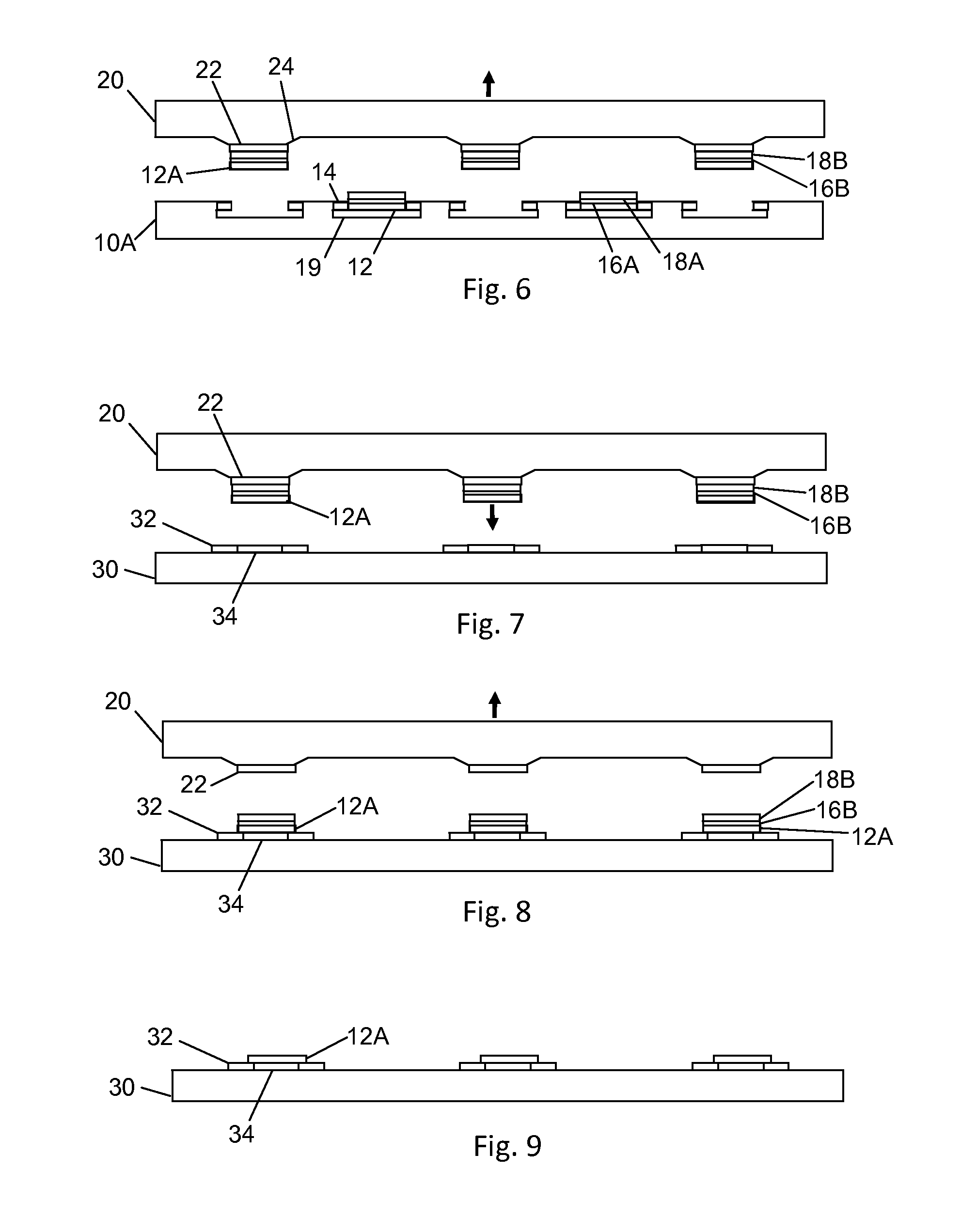
[0055]In a fourth embodiment, the target substrate 30 includes mesas 24 upon which semiconductor dice 12A are deposited using the substantially planar magnetic transfer stamp 20 of the previous alternative embodiment.

[0056]In a fifth alternative embodiment, the tethers 14 connecting semiconductor dice 12 to their host epiwafer substrate 10A are broken by mechanical means (including the application of constant force upon the transfer stamp 20, ultrasonic vibration of the transfer stamp 20 or host epiwafer or substrate 10A, and shock waves or supersonic shock waves propagated through the transfer stamp 20 by means of ultrasonic transducers), the dice 12 being simultaneously held in place for transfer by magnetic forces.

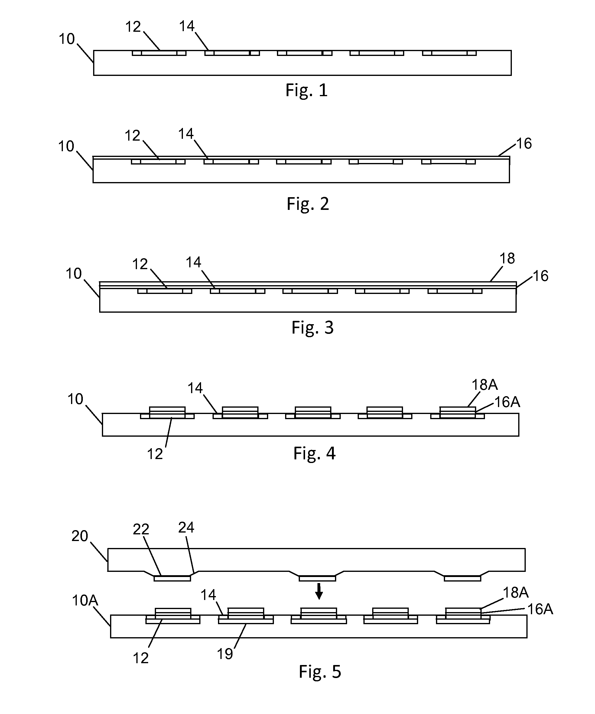
[0057]In a sixth alternative embodiment and referring back to FIG. 5, the transfer stamp 20 has mesas 24, which are coated with a ferromagnetic coating 22. The ferromagnetic coating 22 may be selectively magnetized or demagnetized using a mechanically positioned magneti...

ninth embodiment

[0062]In a ninth embodiment, the electrical contacts of the semiconductor dice 12A are comprised of a ferromagnetic alloy.

[0063]In a tenth alternative embodiment, the semiconductor dice 12A are directly transferred from the source substrate 10A to the target substrate 140 as indicated inFIGS. 14 and 15. Semiconductor dice 12A are attached to source substrate 10A by tethers 14. The target substrate 140 with magnetized mesas 142 is brought into conformal contact with the host substrate 140 whereupon selected semiconductor dice 12A are detached from tethers 14 and transferred to mesas 142 when the host substrate 10A and target substrate 140 are separated. The mesas 142 may then be demagnetized, or if they contain solenoids, de-energized.

[0064]In an eleventh alternative embodiment the magnetic field that is generated is designed such that both location and orientation of the semiconductor dice will hold during the transfer process from source substrate through target substrate. In one e...


PUM


Abstract

Releasable semiconductor dice are deposited with a magnetic layer and held by magnetic forces to a magnetic or electromagnetic transfer stamp for the transfer of the dice from a host substrate directly or indirectly to a target substrate.

Description

[0001]This patent application claims the benefit of U.S. provisional application Nos. 61 / 287,445, 61 / 287,797 and 61 / 375,127, respectively filed Dec. 17, 2009, Dec. 18, 2009 and Aug. 19, 2010. The disclosures of said provisional applications are hereby incorporated herein by reference thereto.TECHNICAL FIELD[0002]The subject matter of the present invention is directed generally to the manufacture of circuits with transferable semiconductor dice and, more particularly, is concerned with a method and magnetic transfer stamp for transferring semiconductor dice from a host substrate to a target substrate using magnetic (or electromagnetic) transfer printing techniques.BACKGROUND ART[0003]Illumination based on semiconductor light sources, such as light-emitting diodes (LEDs), offers an efficient and long-lived alternative to fluorescent, high-intensity discharge and incandescent lamps. Many LED light sources employ high powered LEDs, which pose thermal management problems and other relate...

Claims


Application Information

Patent Timeline
IPC IPC(8): H01L21/50
CPCH01L21/6835H01L24/75H01L2924/1461H01L2924/0133H01L2924/0132H01L2924/0665H01L2924/01075H01L2924/01066H01L2924/01033H01L2924/01019H01L2924/01006H01L2924/01005H01L2224/2919H01L2924/19041H01L2924/14H01L2924/01105H01L2924/01094H01L2924/01088H01L24/83H01L24/95H01L2221/6835H01L2221/68368H01L2221/68381H01L2224/83192H01L2224/838H01L2924/01011H01L2924/01012H01L2924/01013H01L2924/01018H01L2924/01029H01L2924/01049H01L2924/01058H01L2924/0106H01L2924/01064H01L2924/01073H01L2924/01078H01L2924/00H01L2924/01027H01L2924/01028H01L2924/01026H01L2224/95001H01L2224/95136
Inventor ASHDOWN, IANSPEIER, INGOSHEEN, CALVIN WADESCHICK, PHILIPPE MICHAEL
Owner COOLEDGE LIGHTING
Why Eureka
Try Eureka