Multi-stage reconfiguration device and reconfiguration method, logic circuit correction device, and reconfigurable multi-stage logic circuit

Inactive Publication Date: 2011-06-23
NAT UNIV CORP KYUSHU INST OF TECH (JP)
View PDF2 Cites 4 Cited by
  • Summary
  • Abstract
  • Description
  • Claims
  • Application Information

AI Technical Summary

Benefits of technology

[0173]As described above, according to the device to reconfigure multi-level logic networks of the present invention, the reconfiguration of the multi-level logic network configured by pq elements following its logic modification can be performed in a short time. In addition, the reconfiguration processing can be performed in a short time with a small computation amount, and a small memory capacity suffices for reconfiguration calculation. Thus, the circuit can be imbedded into a chip as a dedicated circuit.
[0174]Furt

Problems solved by technology

However, a development cost for the ASIC is high, and its modification requires a lot of time and money.
On the other hand, an FPGA (Field Programmable Gate

Method used


Image

  • Multi-stage reconfiguration device and reconfiguration method, logic circuit correction device, and reconfigurable multi-stage logic circuit
  • Multi-stage reconfiguration device and reconfiguration method, logic circuit correction device, and reconfigurable multi-stage logic circuit
  • Multi-stage reconfiguration device and reconfiguration method, logic circuit correction device, and reconfigurable multi-stage logic circuit

Examples


Example

First Embodiment

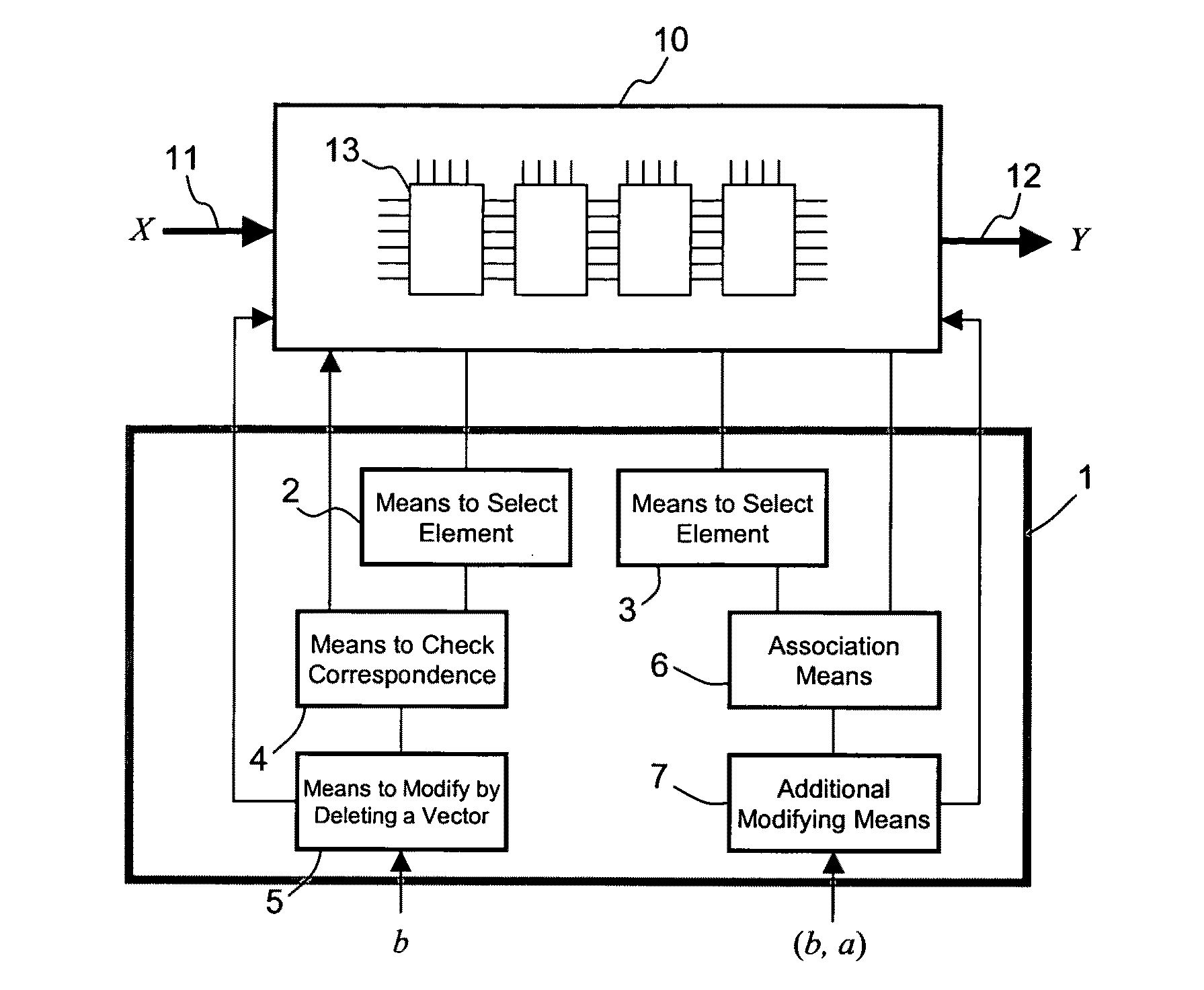
[0222]FIG. 5 shows the configuration of a reconfigurable multi-level logic network according to a first embodiment of the present invention. This reconfigurable multi-level logic network is configured as a system that combines a multi-level logic network 10 and a reconfiguration device 1. The reconfiguration circuit 1 is a device for reconfiguring the multi-level logic network 10 along with logic modification of the multi-level logic network 10.

[0223]The multi-level logic network 10 is a logic circuit for operating an objective logic function F(X) with an input variable X. The multi-level logic network 10 includes plural pq elements 13. Each pq element 13 stores an LUT of a subfunction obtained by functional decomposition of the objective logic function F(X). In addition, the pq elements 13 are connected in circuit according to a connection relation of inputs and outputs of each subfunction. The multi-level logic network 10 may be configured using an LUT cascade circ...

Example

Example 5

[0260]An address generation function F(X) involving five variables as shown in Table 5 is explained.

TABLE 5

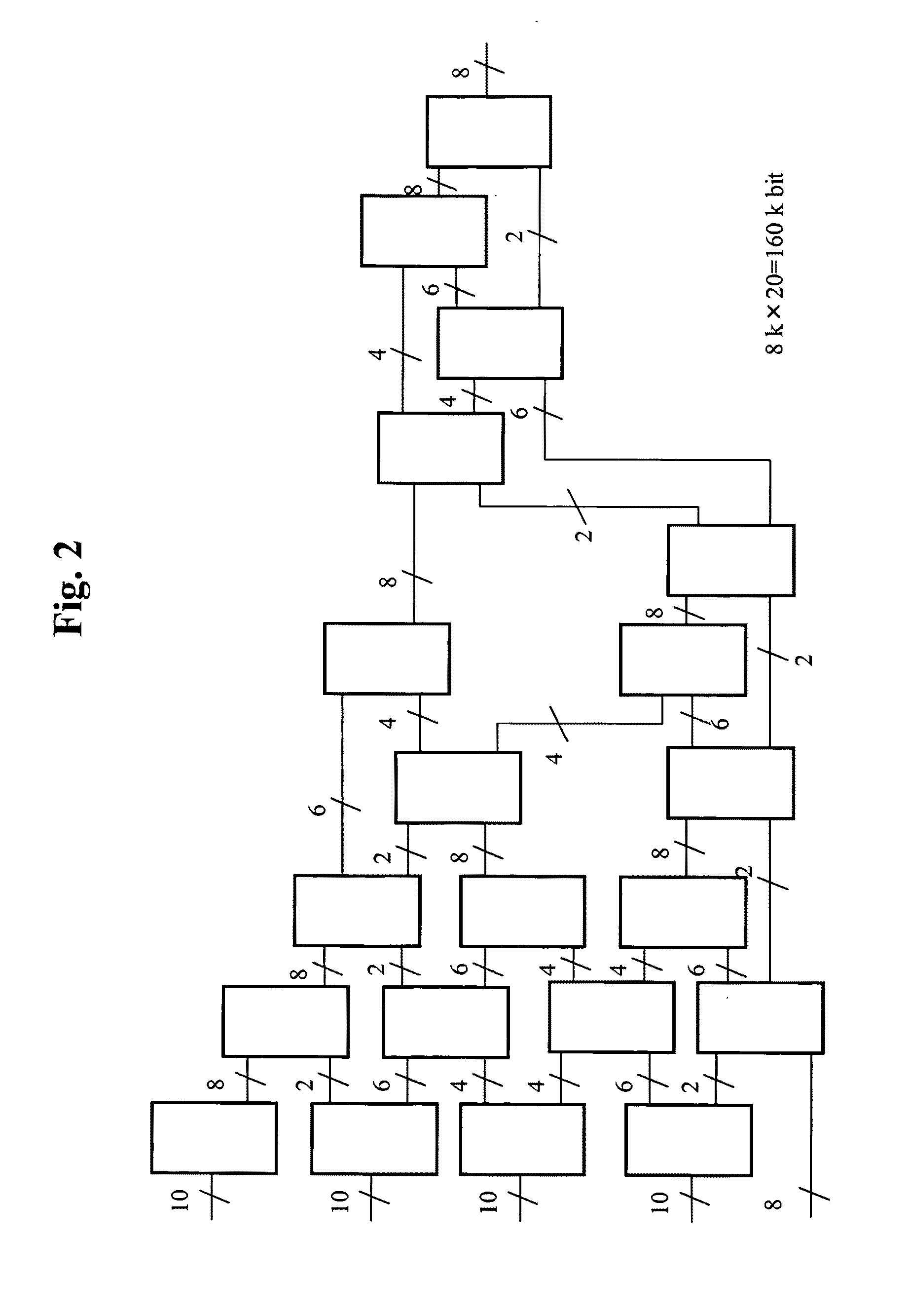
[0261]Functional decomposition {F(X)=G(H(X1), X2)} is executed on partition X of the input variable X; partition X=(X1, X2), X1=(x5, x4, x3, x2), X2=(x1). As a result, the address generation function F(X) is obtained using an LUT cascade logic circuit including two pq elements as shown in FIG. 9. In this example, truth tables of subfunctions H and G are Tables 6 and 7. The truth table (Table 6) of the subfunction H is stored as an LUT in a pq element on the input side. Further, the truth table (Table 7) of the subfunction G is stored as an LUT in a pq element on the output side. Numerical values on the left of each row in Tables 6 and 7 each indicate an index of a registered vector in each row.

TABLE 6TRUTH TABLE FOR FUNCTION H

TABLE 7TRUTH TABLE FOR FUNCTION G

[0262]A registered vector b7 {b7=(x5 x4 x3 x2 x1)=(11001)} of the address generation function F(X) is added. Tab...

Example

Second Embodiment

[0271]FIG. 10 shows the configuration of a device to modify logic networks 20 according to a second embodiment of the present invention. In FIG. 10, a main logic circuit 30 is a logic circuit subjected to logic modification, which is a memory configured as a specific LSI (ASIC), a CPU, or the like. It is assumed that an input variable of the main logic circuit 30 is {X=(x1 x2 . . . xn)(εBn, B={0, 1})}, an output variable thereof is {Q=Q(X)=(q1 q2 . . . qm) (εBm)}, and an output variable modified with the device to modify logic networks 20 is {Q′=(q1′ q2′ . . . qm′) (εBm)}. The main logic circuit 30 operates an objective logic function Q(X) for the input variable X.

[0272]The device to modify logic networks 20 changes an output vector Q(bi) of the main logic circuit 30 corresponding to a particular object input vector bi among input vectors b applied as the input variable X, to a modification output vector Q′(bi). The device to modify logic networks 20 includes an add...


PUM


Abstract

To provide a device to reconfigure multi-level logic networks, which enable logic modification and reconfiguration of a multi-level logic network with small circuit area and low-power dissipation in a simple manner. For example, in the case of reconfiguring a multi-level logic network following logic modification for deleting an output vector F(b) of an objective logic function F(X) corresponding to an input vector b, unmodified pq elements are selected one by one from the nearest pq element EG to an output side. At this time, among output values of pq elements closer to an input side than selected pq elements, output values corresponding to the input vector, which equal an output value corresponding to any input variable X other than the input vector b are considered modified and thus not selected. Then, a selected output value corresponding to the input vector b is rewritten to an “invalid value”.

Description

TECHNICAL FIELD[0001]The present invention relates to a device to reconfigure multi-level logic networks that is logically designed through repetitive functional decomposition of any logic function, and a device to modify logic networks using the same.BACKGROUND ART[0002]A general logic circuit is configured using a special LSI (ASIC: Application Specific Integrated Circuit). However, a development cost for the ASIC is high, and its modification requires a lot of time and money. On the other hand, an FPGA (Field Programmable Gate Array) having simple logic configuration has been developed but is unsatisfactory in terms of power reduction and performance under present circumstances.[0003]To that end, in general, the ASIC is designed with any extra logic circuit being previously incorporated thereinto to enable modification. This design can deal with a minor functional change flexibly to some extent.[0004]A device disclosed in, for example, Patent Document 1 is well-known as a device ...

Claims


Application Information

Patent Timeline
IPC IPC(8): G06F15/76G06F9/30
CPCH03K19/1733
Inventor SASAO, TSUTOMUISHIDA, KAZUTO
Owner NAT UNIV CORP KYUSHU INST OF TECH (JP)
Why Eureka
Try Eureka