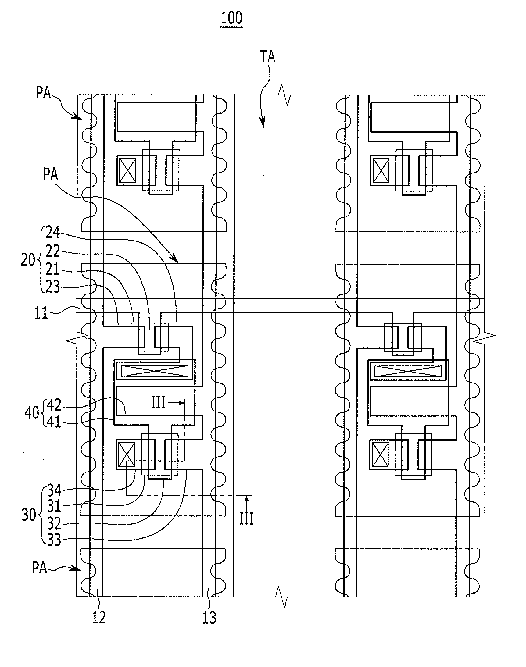
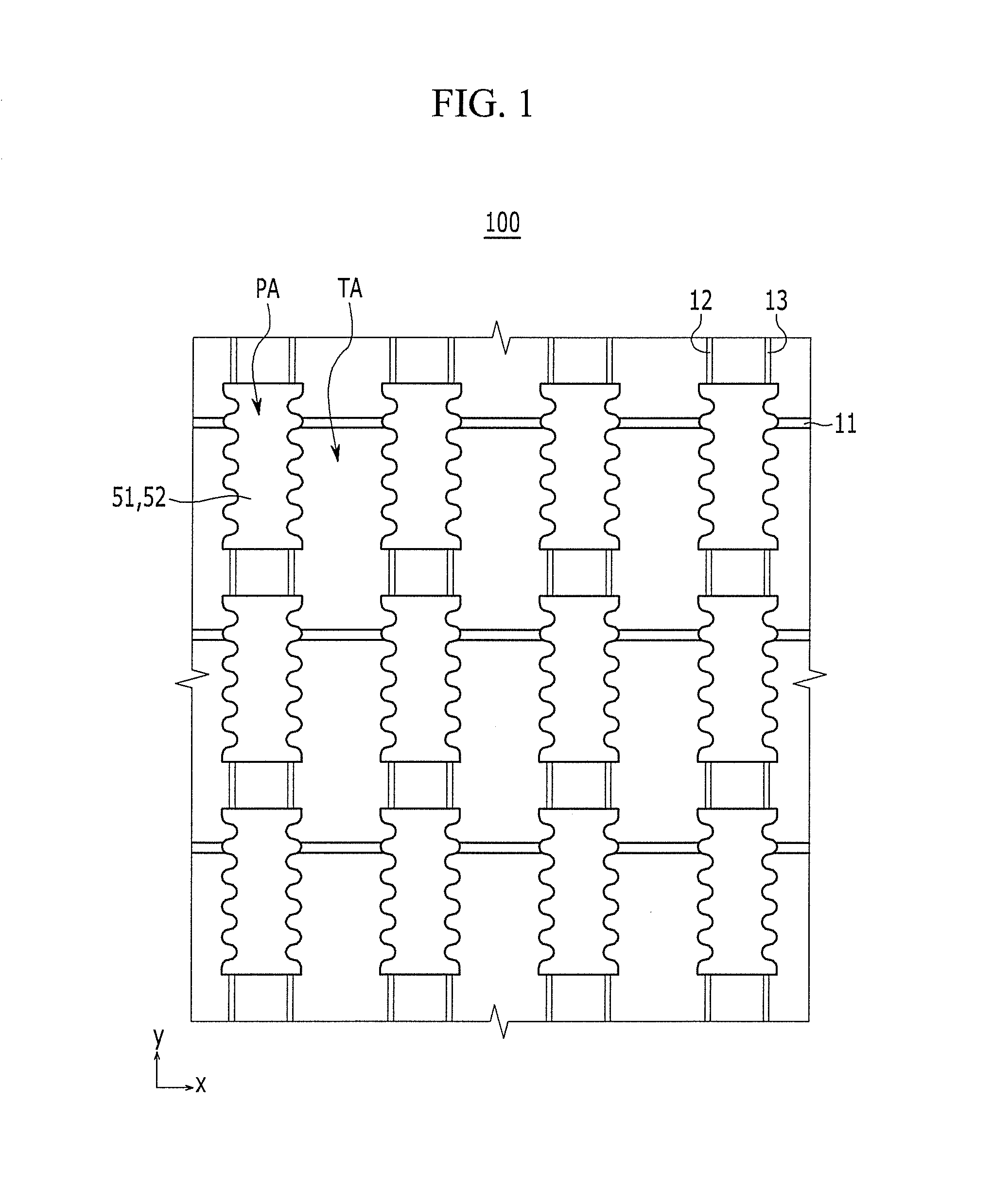
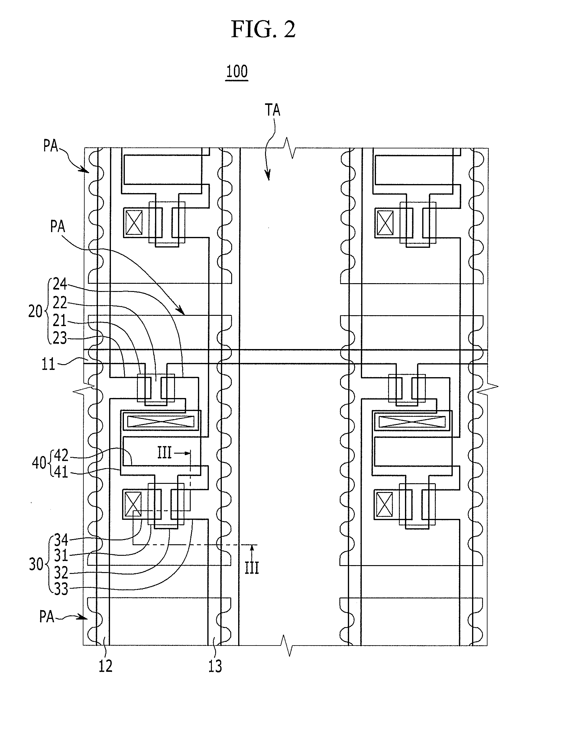
Display device

Active Publication Date: 2011-07-07
SAMSUNG DISPLAY CO LTD
View PDF5 Cites 47 Cited by
  • Summary
  • Abstract
  • Description
  • Claims
  • Application Information

AI Technical Summary

Benefits of technology

[0025]According to the exemplary embodiments, diffraction interference of light passing through the display device can be suppressed by weakening or substantially eliminating periodicity of the width of the transparent area. Theref

Problems solved by technology

Thus, multiple-image distortion occurs when the pixel areas are in the switch-off state, and the image distortion de

Method used


Image

  • Display device
  • Display device
  • Display device

Examples


experimental example 1

Comparative Example

[0102]In a display device of Experimental Example 1, a transparent area has a single horizontal width, and the horizontal width of a pixel area in this experiment is 102 μm and the horizontal width of the transparent area is 50 μm.

[0103]FIG. 10 is a graph showing a simulation result of a diffracted image measured with the display device of Experimental Example 1.

[0104]In the graph of FIG. 10, the vertical axis denotes a brightness ratio of the diffracted image, which is a ratio of brightness I of a diffracted image with respect to brightness IO of an image (for convenience, referred to as “one-transmission image”) that is transmitted without being diffracted. The horizontal axis in the graph denotes a relative distance of the diffracted image, which is a distance of the diffracted image with respect to the one-transmission image. Here, the zero point in the graph indicates a location of the one-transmission image. In the graph, H_R, H_G, and H_B respectively repre...

experimental example 2

Exemplary Embodiment 1

[0106]FIG. 11 is an enlarged view of portions of a pixel area and a transparent area of a display device of Experimental Example 2.

[0107]In the display device of Experimental Example 2, a long side of the pixel area PA is shaped with alternately arranged semi-circular recess portions 54 and semi-circular convex portions 55. The radius r of the semi-circle applied in the experiment is 10 μm, and the maximum horizontal width s1 and the minimum horizontal width s2 of a transparent area TA are 70 μm and 30 μm, respectively.

[0108]FIG. 12 is a graph showing a simulation result of a diffracted image measured with the display device of Experimental Example 2.

[0109]Referring to FIG. 12, it is observed that a diffracted image having a brightness of less than 6% with respect to the brightness of the one-transmission image appears at a location within 2.5 cm from the zero point on the horizontal axis when an observer is located 1 m in front of the display device of Experim...

experimental example 3

Exemplary Embodiment 2

[0110]FIG. 13 is an enlarged view of a portion of a pixel area in a display device of Experimental Example 3.

[0111]In the display device of Experimental Example 3, a long side of a pixel area PA is shaped with alternately arranged rectangular recess portion 541 and rectangular convex portion 551. A horizontal width a and a vertical width b of the recess portion 541 and the convex portion 551 applied in the experiment are respectively 20 μm, and the maximum horizontal width s3 and the minimum horizontal width s4 of a transparent area TA are 70 μm and 30 μm, respectively.

[0112]FIG. 14 is a graph showing a simulation result of a diffracted image measured with a display device of Experimental Example 3.

[0113]Referring to FIG. 14, it is observed that a diffracted image having a brightness of less than 8% with respect to the brightness of the one-transmission image appears at a location within 2.5 cm from the zero point on the horizontal axis when an observer is loca...


PUM


Abstract

A display device includes: i) a substrate member having a transparent area and a plurality of pixel areas, the pixel areas being spaced apart from each other along a first direction and a second direction, the transparent area located between the pixel areas, the second direction being perpendicular to the first direction; and ii) an emission layer located at each of the pixel areas. Among the plurality of pixel areas, a width of the transparent area along the first direction between two pixel areas varies along the second direction. The first direction may be the horizontal direction of a screen realized by the substrate member, the second direction may be a vertical direction, and the emission layer may have a width along the horizontal direction that varies along the vertical direction.

Description

CROSS-REFERENCE TO RELATED APPLICATIONS[0001]This application claims priority to and the benefit of Korean Patent Application No. 10-2010-0000207 filed in the Korean Intellectual Property Office on Jan. 4, 2010, the entire content of which is incorporated herein by reference.BACKGROUND[0002]1. Field[0003]An aspect of embodiments according to the present invention relates generally to a display device.[0004]2. Description of the Related Art[0005]An organic light emitting diode (OLED) display and a field emission display are self-emission display devices, and a transparent display device can be manufactured using the self-emission display device. In further detail, in the self-emission display device, a user can view an image of an object located at the opposite side (i.e., the opposite side of the user with respect to the display device) of the display device when a plurality of pixel areas is formed at a distance from each other with a transparent area between the pixel areas.[0006]...

Claims


Application Information

Patent Timeline
IPC IPC(8): H01L51/52
CPCH01L27/326H01L27/3246H10K59/121H10K59/122H10K50/828
Inventor PARK, CHAN-YOUNGKIM, BEOM-SHIK
Owner SAMSUNG DISPLAY CO LTD
Why Eureka
Try Eureka