
Force Feedback Leveling of Tip Arrays for Nanolithography

a technology of nanolithography and tip array, which is applied in the direction of force/torque/work measurement apparatus, instruments, photomechanical apparatus, etc., can solve the problem that the optical method of leveling is not ideal, and the best optical leveling technique cannot resolve less than a 0.02° differen

Active Publication Date: 2011-07-07
NORTHWESTERN UNIV
View PDF16 Cites 14 Cited by
  • Summary
  • Abstract
  • Description
  • Claims
  • Application Information

AI Technical Summary

Benefits of technology

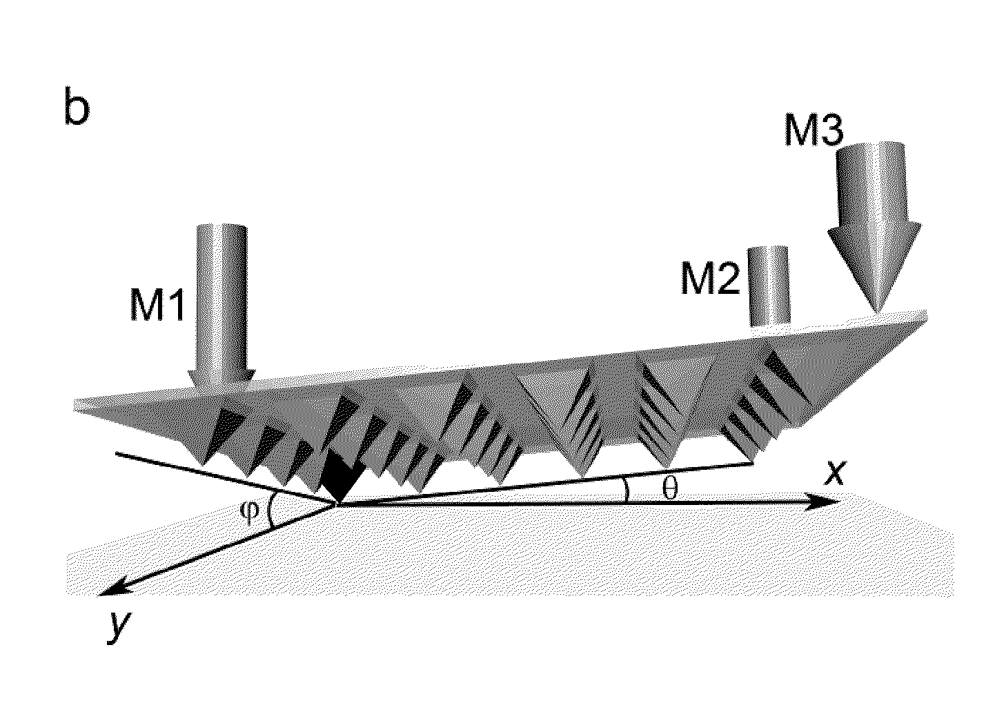
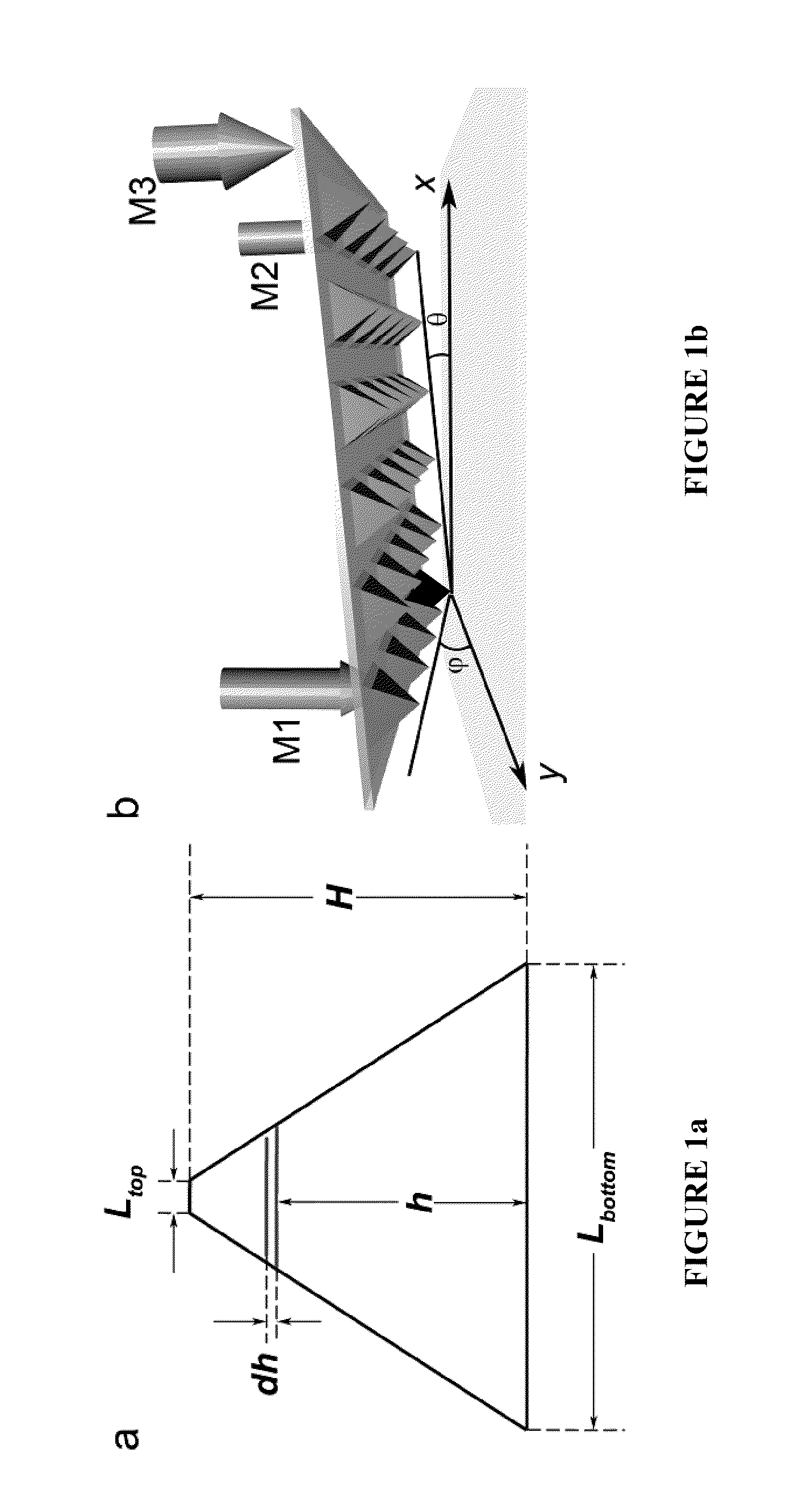
[0010]In accordance with an embodiment of the disclosure, a method of leveling a pen array includes (a) contacting a pen array with a surface and measuring a total force exerted on the surface by the pen array, wherein the surface has first and second axes, the first and second axes being parallel to the surface and perpendicular to one another. The pen array comprises a plurality of tips fixed to a common substrate layer, the tips and the common substrate layer being formed from an elastomeric polymer or elastomeric gel polymer, and the tips having a radius of curvature of less than about 1 μm, and the pen array is disposed at a fir

Problems solved by technology

There are major challenges in transitioning a contact printing tool based upon pyramidal arrays from the micro- or macroscale to the nanoscale, including tip-substrate alignment, ink diffusion control, lateral control over feature spacing, and feature size control.
A challenge that remains for PPL is finding a method to obtain precise leveling between the tip array and the substrate surface.
The inability to produce uniform features of large arrays limits the applicability of PPL to patterning small areas rather than full wafers.
However, this optical method of leveling is not ideal, and features produced by widely separated pens have different edge lengths because of misalignment not identified by optical leveling that is amplified over large distances.
In general, the best optical leveling techniques cannot resolve less than a 0.02° difference in angle between the planes defined by the tip array and the substrate, respectively.
This imprecision results in significant variations in feature edge length.
Additionally, optical leveling requires the use of transmitted light, which limits the array architecture and the materials that can be used to fabricate the pen arrays.

Method used


Image

  • Force Feedback Leveling of Tip Arrays for Nanolithography
  • Force Feedback Leveling of Tip Arrays for Nanolithography
  • Force Feedback Leveling of Tip Arrays for Nanolithography

Examples


example 1

Leveling a Polymer Pen Array

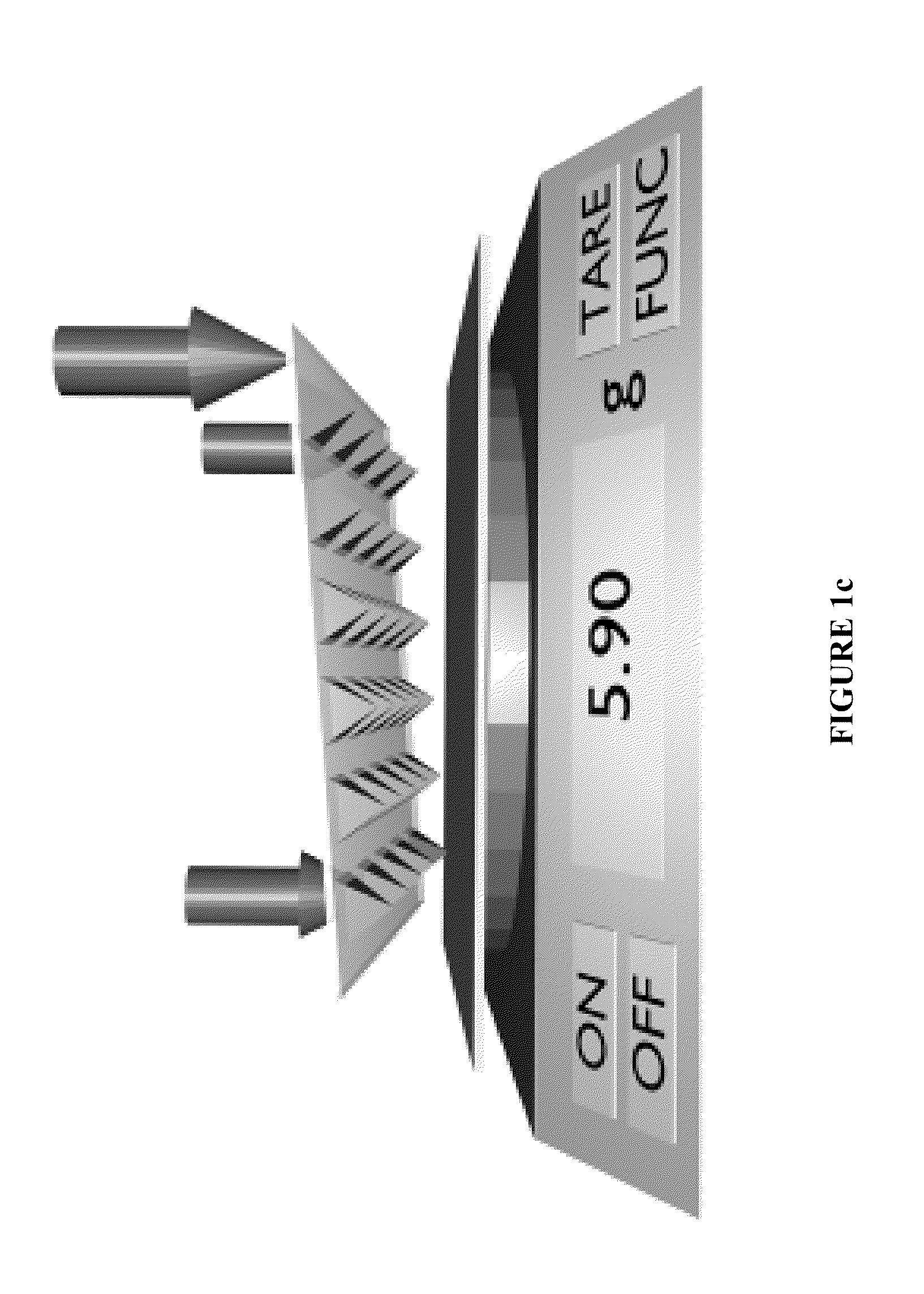
[0133]A method of leveling in accordance with an embodiment of the disclosure was tested using a PPL pen array mounted onto an NSCRIPTOR (NanoInk, Inc.) nanolithography platform. The polymer pen array was 1 cm2, and included approximately 10000 pens, with a spacing D between tips of about 80 μm. A 25 nm thermally evaporated Au thin film with a 5 nm Ti adhesive layer on a S / SiOx substrate was mounted on a force sensor (Ohaus, PS121) having a sensitivity of 0.1 mN.

[0134]The polymer pen array was leveled using a method in accordance with an embodiment of the disclosure. Specifically, the polymer pen array was brought into contact with the surface by extending the z-piezo and the total force was subsequently measured. The polymer pen array was tilted to vary φ while holding θ constant and the total force was again measured upon a Z0 of 12 μm until a local maximum of total force was measured. Referring to FIG. 4a, the measured values of total force were plotte...

example 2

Printing with a Leveled Polymer Pen Array

[0135]Patterns of MHA on Au were written at different values of total force by adjusting θ and φ from the level position. The pens were inked with 16-mercaptohexadecanoic acid (MHA), which can form a self-assembled monolayer (SAM) on a Au surface. A 25 nm thermally evaporated Au thin film with a 5 nm Ti adhesive layer on a S / SiOx substrate was mounted on a force sensor (Ohaus, PS121) having a sensitivity of 0.1 mN. The level position was determined as described in Example 1. The global maximum of total force occurred at 36 mN, and MHA dots were written on the substrate by extending the z-piezo to 10 μm, resulting in patterns in which a single dot was written by each pen in the array (FIG. 5a). The motors were adjusted to a value of (θ, φ)=(0.01, 0), which corresponded to a total force of 33.6 mN, and a pattern of MHA dots was written on the substrate (FIG. 5b). Finally the motors were adjusted to a value of (θ, φ)=(−0.01, 0), which correspond...


PUM


Abstract

A method of leveling a polymer pen array includes contacting a pen array with a surface and measuring a total force exerted on the surface by the pen array, the pen array being disposed at a first angle with respect to a first axis of the surface and a second angle with respect to a second axis of the surface; tilting one or both of the pen array and the surface to vary the first and second angles of the pen array with respect to the surface; measuring the total force exerted by the tilted pen array on the surface; and repeating the tilting and measuring steps until a global maximum of the total force exerted on the surface by the pen array is measured, thereby determining first and second angles which correspond to a leveled position of the pen array with respect to the surface.

Description

CROSS REFERENCE TO RELATED APPLICATIONS[0001]The benefit under 35 U.S.C. §119(e) of U.S. Provisional Patent Application Nos. 61 / 267,382 filed Dec. 7, 2009, and 61 / 292,444 filed Jan. 5, 2010, is hereby claimed, and their entire disclosures are incorporated herein by reference.STATEMENT OF GOVERNMENT INTEREST[0002]This invention was made with government support under grant number N66001-08-1-2044 awarded by the Department of Defense (DARPA) and under grant number EEC-0647560 awarded by the National Science Foundation (NSEC). The government has certain rights in the invention.BACKGROUND[0003]1. Field of the Invention[0004]The invention is generally directed to a method of leveling a pen array, and more particularly to a method of leveling a pen array using a force generated between the pen array and a surface being contacted by the pen array.[0005]2. Brief Description of Related Technology[0006]Polymer pen lithography (PPL) is a molecular printing method that combines the advantages of...

Claims


Application Information

Patent Timeline
IPC IPC(8): B05D5/00B05D1/28G01L1/06B82Y99/00
CPCG03F7/0002
Inventor MIRKIN, CHAD A.LIAO, XINGBRAUNSCHWEIG, ADAM B.
Owner NORTHWESTERN UNIV
Learn More