Nanolithography methods and products therefor and produced thereby

Inactive Publication Date: 2005-09-01
NORTHWESTERN UNIV
View PDF2 Cites 19 Cited by
  • Summary
  • Abstract
  • Description
  • Claims
  • Application Information

AI Technical Summary

Benefits of technology

[0007] One aspect of the invention provides a method of Dip Pen Lithography (DPN) in which the movement of the molecules to be deposited or patterned on the substrate (the deposition compound or the patterning compound) from the tip to the substrate is controlled by a driving force. The driving force can b

Problems solved by technology

The external opening contains a size-restricted aperture such that a deposition compound cannot succe

Method used


Image

  • Nanolithography methods and products therefor and produced thereby
  • Nanolithography methods and products therefor and produced thereby
  • Nanolithography methods and products therefor and produced thereby

Examples


Embodiment Construction

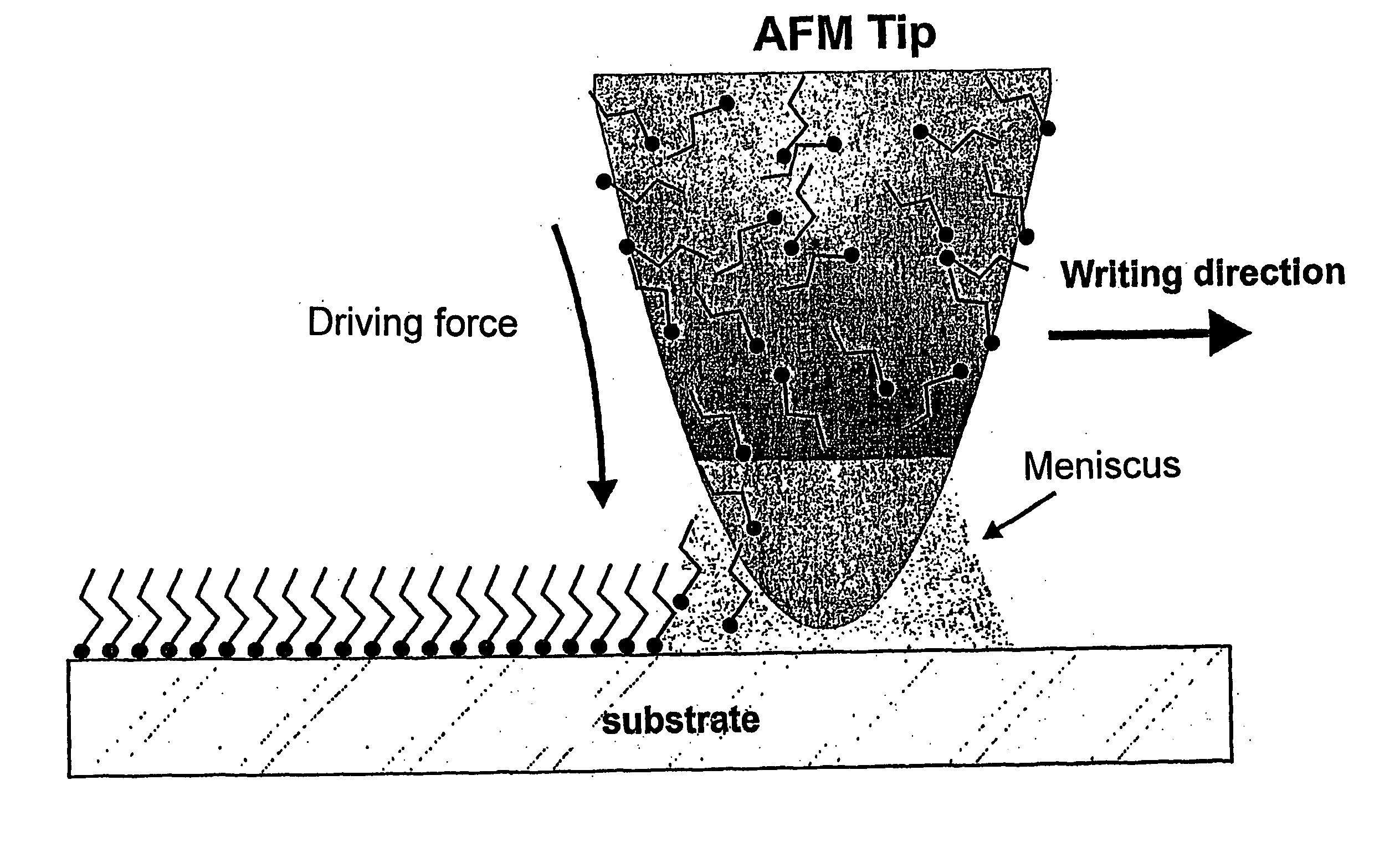
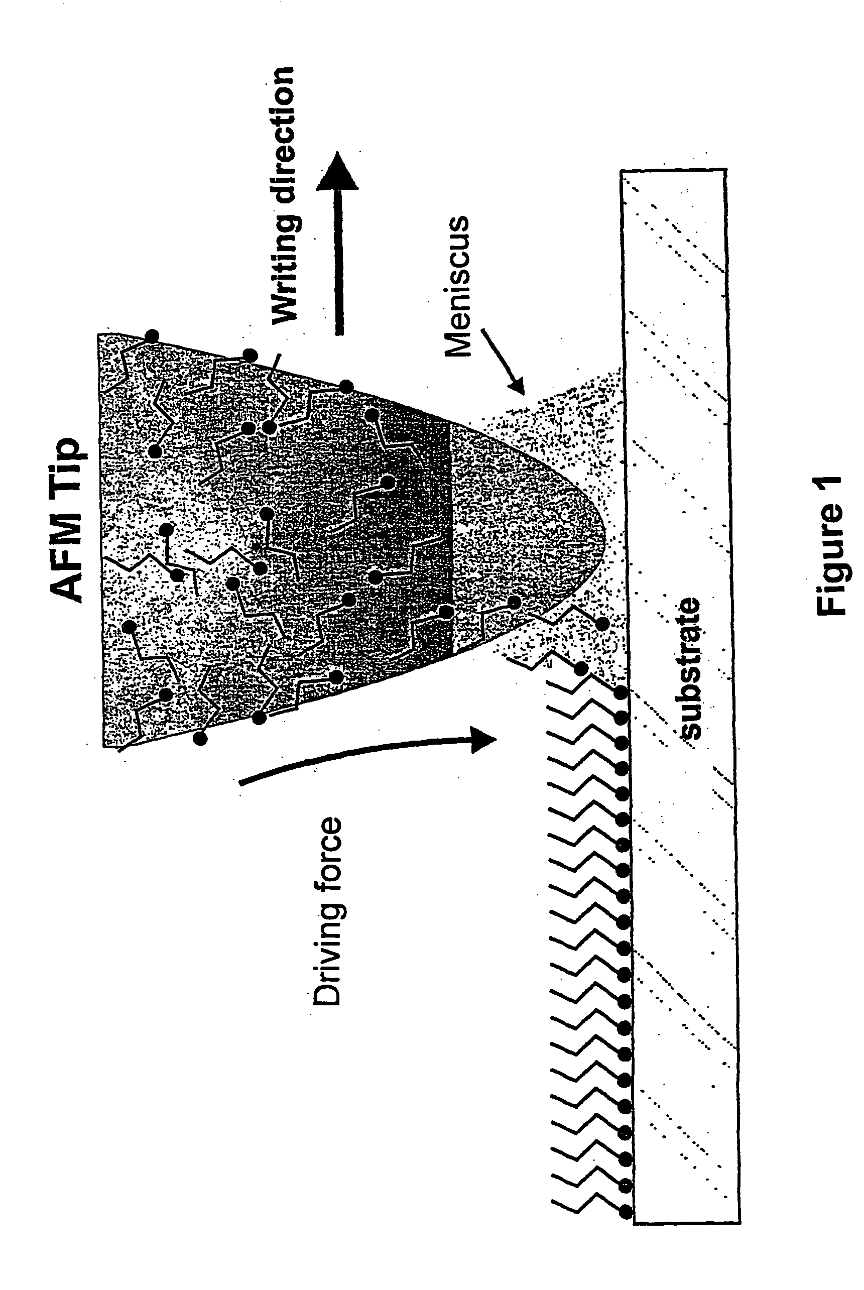
[0016] A. Dip Pen Nanolithography

[0017] The invention provides a method of nanolithogrphy for precisely patterning or depositing molecules on a substrate to form thin film nanostructures. The invention an improved method of DPN in which the rate and extent of the movement of the deposition compound from the tip to the substrate is controlled by a driving force.

[0018] To practice DPN, a scanning probe microscope (SPM) tip is coated with a patterning compound. This can be accomplished in a number of ways. For instance, the tip can be coated by vapor deposition, by direct contact scanning, or by bringing the tip into contact with a solution of the patterning compound.

[0019] The simplest method of coating the tips is by direct contact scanning. Coating by direct contact scanning is accomplished by depositing a drop of a saturated solution of the patterning compound on a solid substrate (e.g., glass or silicon nitride; available from Fisher Scientific or MEMS Technology Application Ce...


PUM

PropertyMeasurementUnit
Thicknessaaaaaaaaaa
Thicknessaaaaaaaaaa
Diameteraaaaaaaaaa

Abstract

In one aspect, a method of nanolithography is provided using a driving force to control the movement of a deposition compound from a scanning probe microscope tip to a substrate. Another aspect of the invention provides a tip for use in nanolithography having an internal cavity and an aperture restricting movement of a deposition compound from the tip to the substrate. The rate and extent of movement of the deposition compound through the aperture is controlled by a driving force.

Description

[0001] This application claims benefit of provisional application No. 60 / 264,550, filed Jan. 26, 2001, the complete disclosure of which is incorporated herein by reference, and is a continuation-in-part of pending application Ser. No. 09 / 477,997 filed Jan. 5, 2000, the complete disclosure of which is incorporated herein by reference.[0002] This invention was made with government support under grant(s) [______] from [______]. The U.S. government has rights in the invention.FIELD OF THE INVENTION [0003] This invention relates to methods of nanolithography and products therefor and produced thereby. BACKGROUND OF THE INVENTION [0004] Lithographic methods are at the heart of modern day microfabrication, nanotechnology and molecular electronics. Microfabrication techniques such as photolithography, microcontact printing, micromachining, and microwriting can produce patterns as small as 100 nm, but the production of sub-100 nm structures still poses a challenge. Amro et al., Langmuir, 16,...

Claims


Application Information

Patent Timeline
IPC IPC(8): B05D1/00B05D1/18B05D1/26B82B3/00G01Q60/00G01Q70/16G01Q80/00G03F7/00G03F7/16
CPCB05D1/007Y10S977/886B05D1/26B82B3/00B82Y10/00B82Y30/00B82Y40/00G01Q80/00G03F7/0002G03F7/165Y10S977/86Y10S977/863Y10S977/857Y10S977/862Y10S977/878Y10S977/882Y10S977/85Y10S977/884Y10S977/885B05D1/185
Inventor MIRKIN, CHAD A.HONG, SEUNGHUNDRAVID, VINAYAK P.
Owner NORTHWESTERN UNIV
Why Eureka
Try Eureka