

Field-assisted micro- and nano-fabrication method
a microfabrication and field-assisted technology, applied in the field of microfabrication and nanofabrication, can solve the problems of not being economically practical to use ebl for and unable to achieve the effect of mass production of sub-50 nm structures
- Summary
- Abstract
- Description
- Claims
- Application Information
AI Technical Summary
Problems solved by technology
Method used
Image

Examples
example 1
The Deposition of 1-octadecanethiol (ODT) to gold (Au) Surfaces
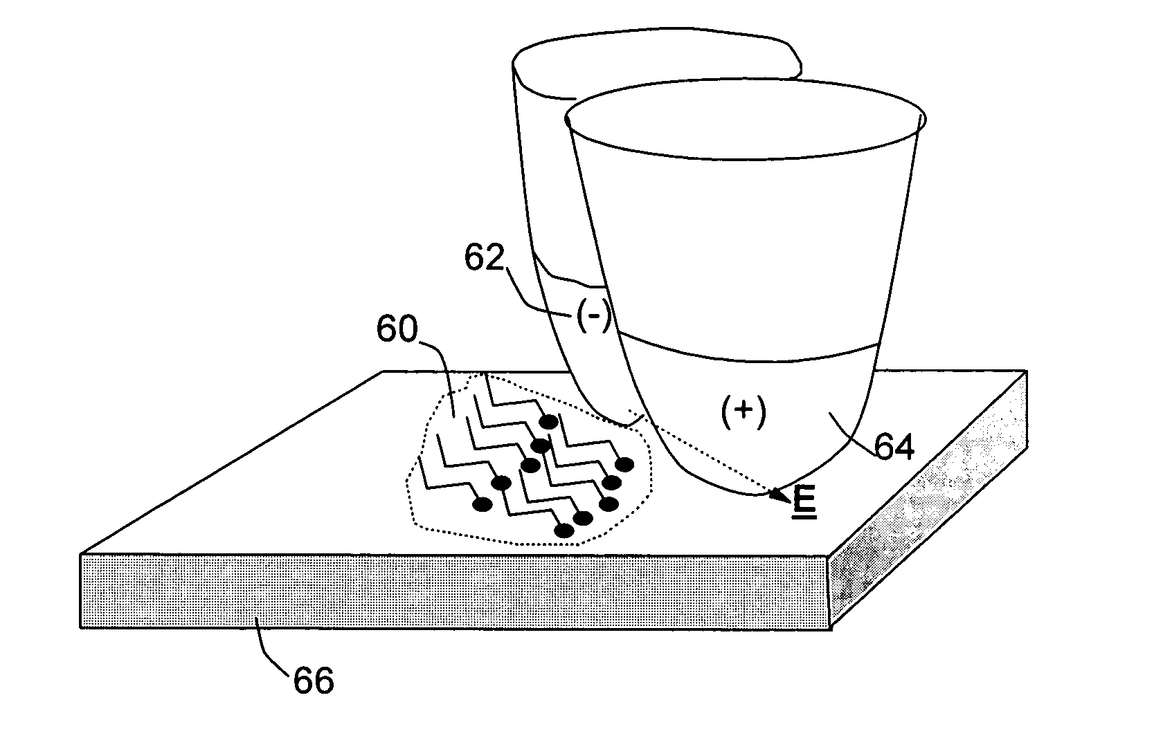
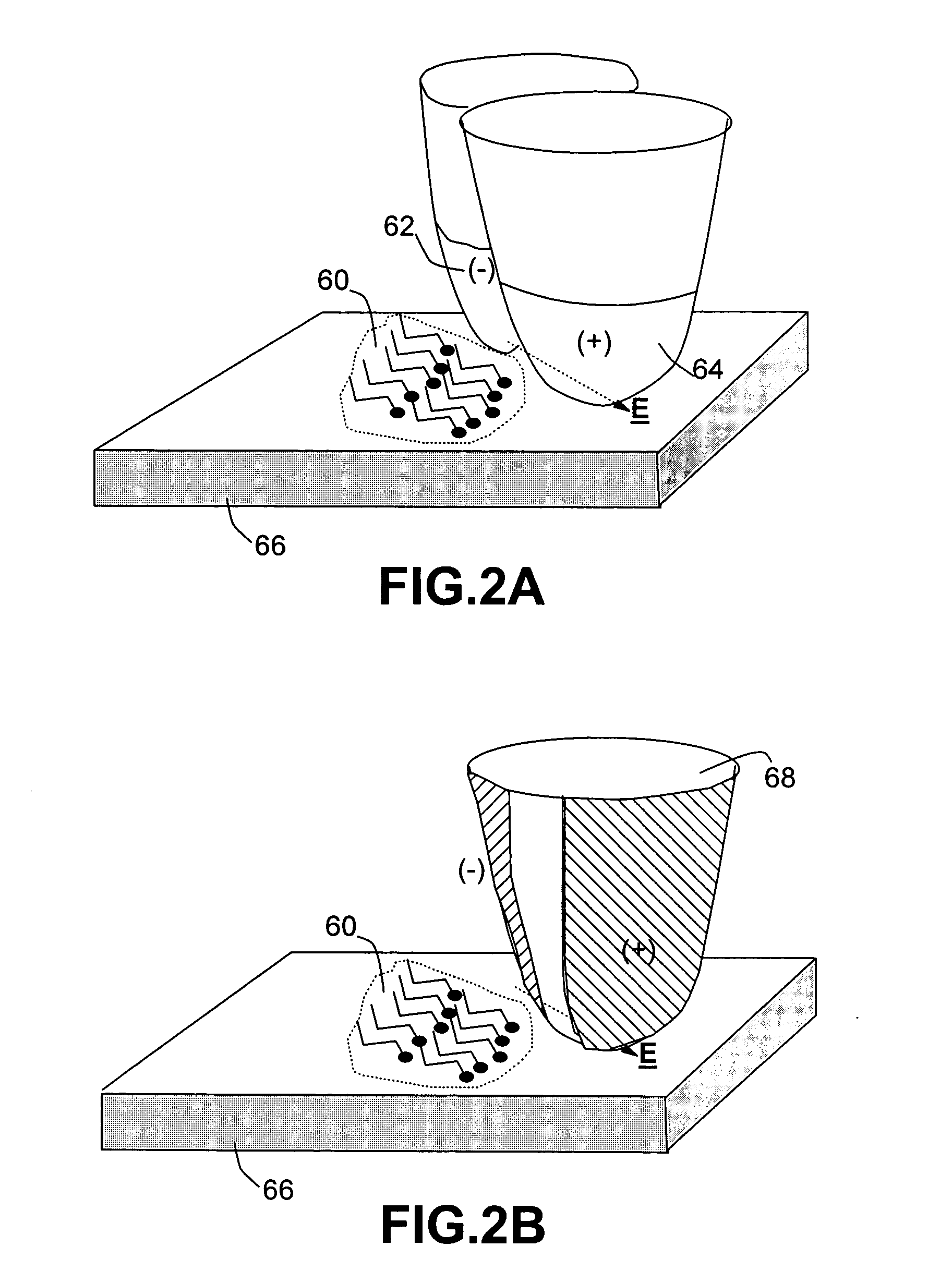
[0026] Example 1 involves deposition of ODT on a gold substrate. The procedure involved bringing an ODT-coated optical fiber tip into contact with a sample surface. The ODT molecules flowed from the fiber tip to the sample by capillary action. An optical fiber tip was sputter-coated with a thin gold electrode of 20 nm thick (the first electrode). The gold-plated fiber tip was then tentatively coated with ODT by dipping the fiber into a saturated solution of ODT in acetonitrile for 1 minute. A second optical fiber tip, coated with gold, serves as the second electrode which, in combination with the first electrode, provides a high electric field along a direction parallel to the line defined by the two tips. The dip pen nano-lithography process involved raster scanning such a tip across a 1 μm×1 μm section of a Au substrate positioned on a nano-positioning stage. Formation of high-quality self-assembled monolayers (SAMs) ...
example 2
[0027] Poly (vinylidene fluoride), PVDF, is a polarizable material which is used herein as an example. The method begins by first dissolving PVDF in a suitable amount of solvent to form a solution. Approximately 4% by weight of PVDF was dissolved in 96% of tricresylphosphate. A capacitor grade PVDF available from Kureha Kagoku Kogko Kabishiki Kaisha was used. Some of the solvent was vaporized to reduce the solvent content of the solution. As shown in FIG. 2B, the solution of PVDF was coated onto a dip pen (such as 68 in FIG. 2B) with additional amount of the solvent being allowed to vaporize The solution was delivered onto a target surface (a quartz) to form a domain of PVDF molecules with a preferred orientation. The procedure was repeated and continued until a PVDF film of a predetermined pattern was deposited. Both the dip pen and the target surface were placed in a suitable vacuum oven. The PVDF solution deposited, in small micrometer- and nanometer-scale regions, was subjected ...
PUM
| Property | Measurement | Unit |
|---|---|---|
| size | aaaaa | aaaaa |
| sizes | aaaaa | aaaaa |
| size | aaaaa | aaaaa |
Abstract
Description
Claims
Application Information