Super-diffraction imaging device for improving resolution based on phase shifting principle and manufacturing method thereof

An imaging device and super-diffraction technology, applied in the field of nano-processing, can solve the problem that super-resolution imaging lithography is difficult to achieve lithography resolution of 40nm and below, and achieve the goal of improving light energy utilization, offsetting energy loss, and increasing focal depth Effect

Active Publication Date: 2011-06-15
INST OF OPTICS & ELECTRONICS - CHINESE ACAD OF SCI
View PDF5 Cites 19 Cited by
  • Summary
  • Abstract
  • Description
  • Claims
  • Application Information

AI Technical Summary

Problems solved by technology

[0004] The technical problem to be solved by the present invention is to provide a phase-shifting super-diffraction imaging device with improved resolution and a manufacturing method thereof, aiming at the problem that the existing super-resolution imaging lith

Method used


Image

  • Super-diffraction imaging device for improving resolution based on phase shifting principle and manufacturing method thereof
  • Super-diffraction imaging device for improving resolution based on phase shifting principle and manufacturing method thereof
  • Super-diffraction imaging device for improving resolution based on phase shifting principle and manufacturing method thereof

Examples


Embodiment Construction

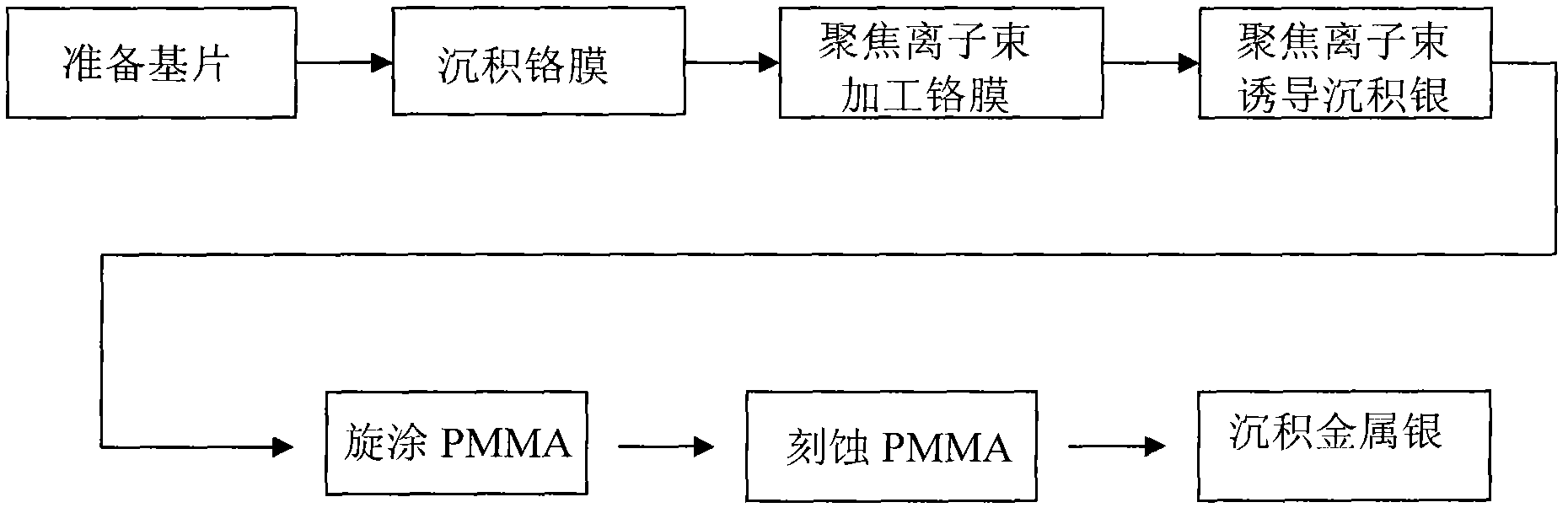
[0032] The present invention will be described in detail below in conjunction with the accompanying drawings and specific embodiments. But the following examples are only limited to explain the present invention, and the protection scope of the present invention should include the entire content of the claims, and those skilled in the art can realize the entire contents of the claims of the present invention through the following examples.

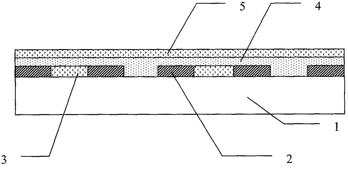
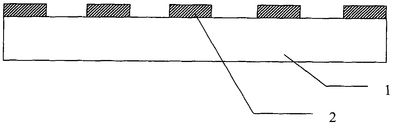
[0033] Embodiment 1 of the present invention is to make a phase-shift mask with a period of 40nm and a line width of 20nm, and the exposure wavelength is 365nm. The mask includes a transparent quartz substrate, a chromium film pattern, and PMMA and metallic silver.

[0034] The mask fabrication steps are as follows figure 2 Shown:

[0035] (1) select quartz to make ultraviolet light transparent substrate;

[0036] (2) Utilize magnetron sputtering to process the chromium film that thickness is 50nm on one side of ultraviolet light trans...


PUM

PropertyMeasurementUnit
Thicknessaaaaaaaaaa
Thicknessaaaaaaaaaa
Thicknessaaaaaaaaaa

Abstract

The invention discloses a super-diffraction imaging device for improving resolution based on a phase shifting principle and a manufacturing method thereof. Adjacent light transmission areas of the super-diffraction imaging device realize phase delay and phase advance respectively by alternately filling two materials with a positive dielectric coefficient and a negative dielectric coefficient and the phase difference modulation of the material thicknesses is enhanced greatly, so that the device is easier to realize a pi phase difference; therefore, the imaging resolution of the device is further improved. The scheme solves the technical difficult problem that a conventional super-diffraction imaging device is difficult to realize the resolution below the line width of 40 nm and has a broad application prospect in super-diffraction imaging and nano-lithography technologies.

Description

technical field [0001] The invention belongs to the technical field of nano-processing, and relates to a super-diffraction imaging device with improved resolution based on a phase-shifting principle and a manufacturing method thereof. technical background [0002] Since Pendry proposed the concepts of "perfect lens" and "superlens" in 2000, surface plasmon-based super-resolution imaging lithography has attracted widespread attention due to its advantages of low cost, high efficiency, and high resolution. In 2005, Xiang.Z. used the "super-lens" to obtain 60nm super-resolution lithography experimentally for the first time under a 365nm light source. New Zealand R.J.Blaikie also made more in-depth research on the super-lens imaging lithography. However, although the "superlens" can break through the diffraction limit, it still limits its resolution due to factors such as loss and scattering. The minimum linewidth obtained by the superlens imaging lithography reported in the lit...

Claims


Application Information

Patent Timeline
IPC IPC(8): G03F7/20G03F1/08G03F1/00G03F1/30
Inventor 王长涛方亮罗先刚刘玲冯沁赖之安杨欢
Owner INST OF OPTICS & ELECTRONICS - CHINESE ACAD OF SCI
Why Eureka
Try Eureka