Inclined PN junction doped structure of silica-based electro-optic modulator

An electro-optic modulator, PN junction technology, applied in instruments, optics, nonlinear optics, etc., can solve the problem of large modulation energy consumption, achieve the effect of overcoming the incompatibility of modulation efficiency and modulation power consumption, and ensuring high-speed modulation performance

Active Publication Date: 2016-04-20
PEKING UNIV
View PDF5 Cites 10 Cited by
  • Summary
  • Abstract
  • Description
  • Claims
  • Application Information

AI Technical Summary

Problems solved by technology

In addition, in the existing finger-junction technology solutions, vertical PN junction doping structures are mostly used, for example, the extension direction of the finger-junction is perpendicular to the core region of the waveguide (such as the rib region higher than the plate region in the ridge waveguide, the sidewall The extension direction of the ridge region higher than the grating region in the grating waveguide), or the doping plane of the PN junction is perpendicular to the plane of the lateral waveguide (such as the slab region of the ridge waveguide, the grating region of the sidewall grating waveguide), to a certain extent The junction area of ​​the PN junction is limited, which leads to large modulation energy consumption

Method used


Image

  • Inclined PN junction doped structure of silica-based electro-optic modulator
  • Inclined PN junction doped structure of silica-based electro-optic modulator
  • Inclined PN junction doped structure of silica-based electro-optic modulator

Examples


Embodiment Construction

[0030] In order to make the purpose, technical solutions and advantages of the embodiments of the present invention clearer, the technical solutions in the embodiments of the present invention will be clearly described below in conjunction with the accompanying drawings in the embodiments of the present invention. Obviously, the described embodiments are the Some, but not all, embodiments are invented. Based on the embodiments of the present invention, all other embodiments obtained by persons of ordinary skill in the art without making creative efforts belong to the protection scope of the present invention.

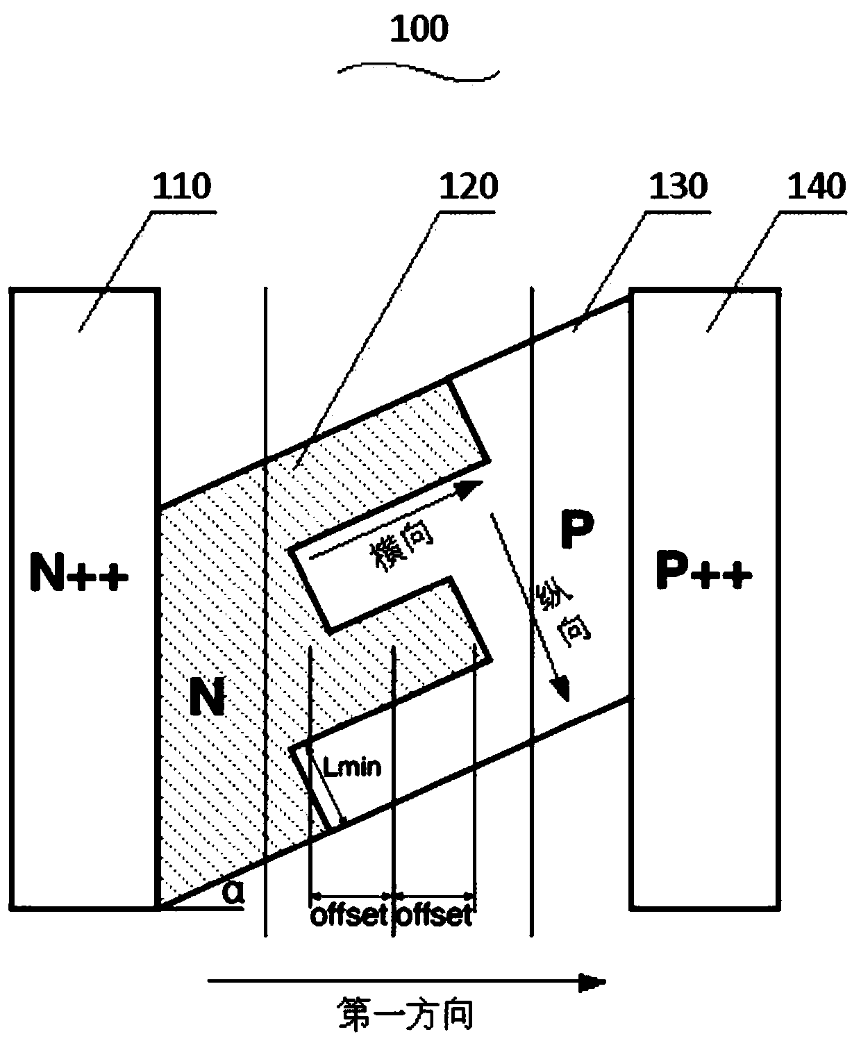
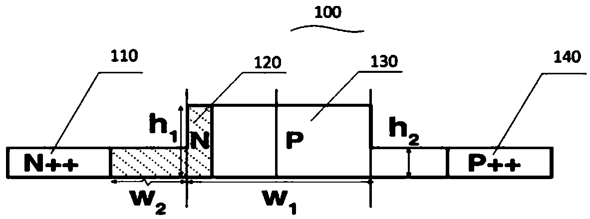
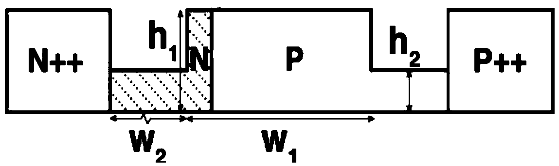
[0031] Figure 1-a , Figure 1-b Respectively show a top view and a schematic cross-sectional view of a silicon-based electro-optic modulator inclined PN junction doping structure according to an embodiment of the present invention; Figure 1-a , Figure 1-b As shown, the doping structure includes:

[0032] Silicon-based electro-optic modulator modulation region waveg...


PUM


Abstract

The invention relates to a doped structure of a silica-based electro-optic modulator. The doped structure comprises a modulation region waveguide of the silica-based electro-optic modulator, wherein the waveguide comprises a first heavily doped region, a second lightly doped region, a third lightly doped region and a fourth heavily doped region in sequence in the first direction; the second lightly doped region and the third lightly doped region form at least one longitudinally inclined PN junction and at least one transversely inclined PN junction, and the longitudinal direction is perpendicular to the transverse direction; a first included angle is formed between the longitudinal direction and the first direction and is larger than 0 degree and smaller than 90 degrees. The doped structure can lower modulation energy consumption while improving modulation efficiency of the silica-based electro-optic modulator, make all doped regions in the core area of the waveguide achieve electrical connection directly through the lateral waveguide, and guarantee high-speed modulation performance of a system.

Description

technical field [0001] The invention relates to the technical field of semiconductors, in particular to an inclined PN junction doping structure of a silicon-based electro-optic modulator. Background technique [0002] With the development trend of speed-up and cost-reduction of communication and interconnection, a large number of communication and interconnection equipment are updated, and silicon-based transceiver systems have begun to be used commercially. However, the system consumes a lot of energy, and the pressure on communication and interconnection infrastructure has increased sharply. The modulator is an important component of the transceiver in the optical communication and optical interconnection system. Its energy consumption is second only to the laser, but the insertion loss of the modulator itself also increases the power consumption budget, so it is an important part of the current efforts to reduce energy consumption. Research object. [0003] Both modulat...

Claims


Application Information

Patent Timeline
Patent Type & Authority Applications(China)
IPC IPC(8): G02F1/025
CPCG02F1/025
Inventor 周治平李心白
Owner PEKING UNIV
Why Eureka
Try Eureka