Fourier laminated microimaging device and method

A technology of Fourier stacking and microscopic imaging, which is applied in microscopes, measuring devices, optics, etc., can solve the problems of low resolution and low efficiency of restoring sample images, and achieve high resolution, easy large-angle illumination, and modulation high efficiency effect

Active Publication Date: 2019-04-05
XI'AN INST OF OPTICS & FINE MECHANICS - CHINESE ACAD OF SCI +1
View PDF3 Cites 10 Cited by
  • Summary
  • Abstract
  • Description
  • Claims
  • Application Information

AI Technical Summary

Problems solved by technology

[0004] In order to solve the technical problems of low efficiency and low resolution of the existing Fourier stack microscopic imaging technology for recovering sample images, the present invention provides a Fourier stack microscopic imaging device and method

Method used


Image

  • Fourier laminated microimaging device and method
  • Fourier laminated microimaging device and method
  • Fourier laminated microimaging device and method

Examples


Embodiment

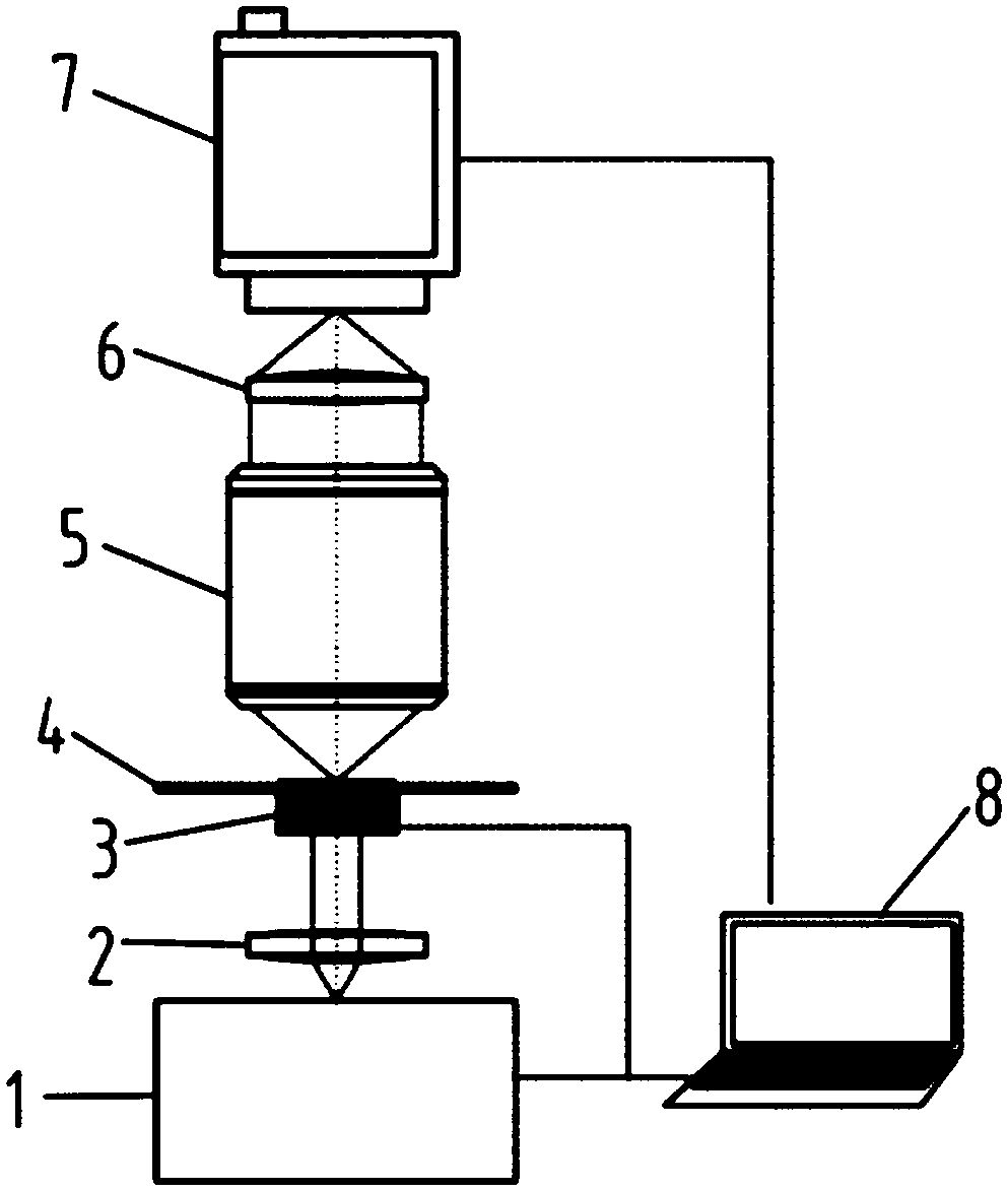
[0102] The liquid crystal beam deflection device 3 adopts a liquid crystal prism;

[0103] The microscopic objective lens 5 adopts a twice achromatic microscopic objective lens, the numerical aperture NA is 0.1, and the objective lens aperture is 15mm;

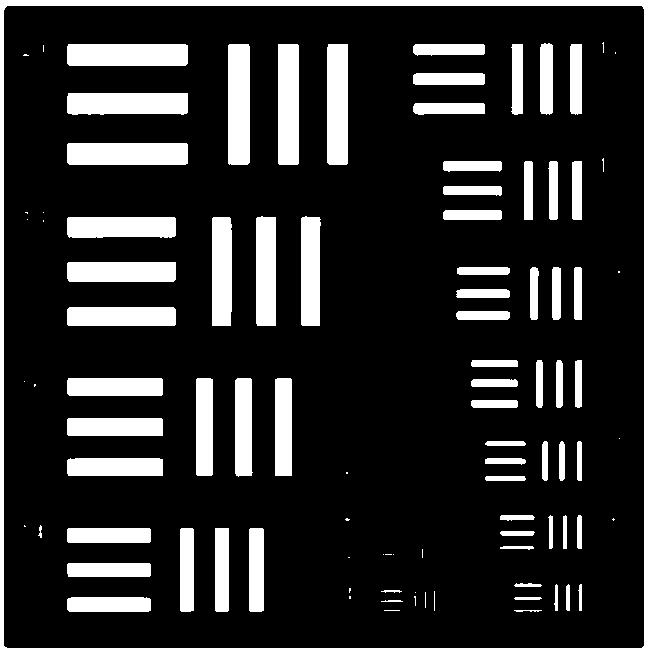
[0104] The sample to be tested (such as figure 2 ) is the USAF1951 standard resolution board;

[0105] Laser 1 selects a red He-Ne laser with a wavelength of 632nm;

[0106] Collimating lens 2 collimates the laser beam to the parallel light;

[0107] Camera 7 uses a CCD sensor with a pixel size of 5.5um;

[0108] The liquid crystal prism is placed close to the bottom of the sample stage 4;

[0109] The desired synthetic numerical aperture NA' is 0.3, and it is necessary to ensure that the spectral overlap ratio = 50%.

[0110] Follow the steps below to implement:

[0111] The first step: determine the beam angle α of each modulation of the liquid crystal prism i,j .

[0112] 1.1 According to N=2NA' / NA, calculate N=6...


PUM


Abstract

In order to solve the technical problems of low efficiency and low resolution of the existing Fourier laminated microimaging technology to recover sample images, the invention provides a Fourier laminated microimaging device and method. The device comprises a computer, and a laser, a collimating lens, a liquid crystal beam deflecting device, a sample stage, a microscope objective, a pipe mirror and a camera, which are sequentially arranged along an optical path from bottom to top; an outgoing beam center of the collimating lens and the center of the liquid crystal beam deflecting device are both coincident with the optical axis of the microscope objective; the liquid crystal beam deflecting device modulates the angle of a beam incident on a sample to be tested according to a computer control instruction; and the beams of two adjacent angles separately illuminate the sample, the diffraction spectrum information obtained on a Fourier plane of the microscope objective has an overlapping ratio greater than or equal to 50%; the camera collects a microscopic image corresponding to each beam angle incident on the sample to be tested according to computer control instruction; and the computer is also used for performing fusion reconstruction on the microscopic images obtained by the camera at different beam angles to obtain a final sample image.

Description

technical field [0001] The invention belongs to the technical field of optical microscopic imaging, and relates to Fourier stacked microscopic imaging technology, in particular to a Fourier stacked microscopic imaging device and method based on liquid crystal beam deflection technology. Background technique [0002] Traditional optical microscopes cannot obtain large field of view and high-resolution images at the same time, and can only obtain the amplitude information of the sample, but cannot obtain the phase information. [0003] In 2013, Zheng from Caltech introduced Fourier stack imaging technology into the field of microscopic imaging for the first time, and realized microscopic imaging technology with high resolution and large field of view at the same time: by placing the LED array at a certain distance below the sample , the thin sample on the sample stage is illuminated by different angles of plane light from different LEDs, on the Fourier plane of the microscope ...

Claims


Application Information

Patent Timeline
Patent Type & Authority Applications(China)
IPC IPC(8): G02B21/06G02B21/36G01N21/00
CPCG01N21/00G02B21/06G02B21/367G02B21/368
Inventor 相萌李创赵意意
Owner XI'AN INST OF OPTICS & FINE MECHANICS - CHINESE ACAD OF SCI
Why Eureka
Try Eureka