Novel ultrananocrystalline diamond probes for high-resolution low-wear nanolithographic techniques

a nanolithography and ultrananocrystalline technology, applied in the field of three-dimensional probes, can solve the problems of limiting the lifetime, accuracy and reproducibility of afm measurements, and high hardness and high coefficient of friction, and achieve the effects of reducing the accuracy of afm measuremen

Inactive Publication Date: 2007-09-27
UCHICAGO ARGONNE LLC
View PDF3 Cites 20 Cited by
  • Summary
  • Abstract
  • Description
  • Claims
  • Application Information

AI Technical Summary

Problems solved by technology

However, AFM, which utilizes probes consisting of micro cantilevers with integrated nano-scale tips generally made of Si or other materials with relatively low hardness and high coefficient of friction, have two main drawbacks.
First, the probes suffer from wear, degradation, and contamination too easily.
This limits the lifetime, accuracy, and reproducibility of AFM measurements.
Second, the nature of the probe's structure itself, a simple fixed-free beam that must be tilted at an angle so that the tip touches the surface first, has several disadvantages structurally, namely: (1) the micro cantilever is difficult to calibrate accurately; (2) the tilt introduces coupling between normal and in-plane forces, rendering mechanical measurements subject to uncertainty and error; and (3) forces are only measured along two axes, namely the vertical direction and the lateral direction (i.e. in-plane, perpendicular to the long axis of the cantilever), but forces in the longitudinal direction (i.e. in-plane, parallel to the long axis of the cantilever) are coupled into the normal force signal.
These techniques require sophisticated probes, such as those employed in nanolithography, arrays for parallel imaging, writing, and data reading / recording, or even more complex tasks such as drilling, cutting, or milling.
The cost of these specialized probes and their functional life, in terms of scanning distance, are strongly competing parameters in their design.
The lifetime of probes is typically shortened by mechanical failure in operation and handling, pickup of material and particles from the samples, and wear.
DLC films are smoother and easier to integrate into more complex fabrication schemes but cannot be made highly conductive.
This technique has the disadvantage that it increases the initial tip radius of the probes (10-20 nm) by the thickness of the diamond film (typically 70-100 nm to achieve full coverage of the substrate); thus, it results in much lower tip sharpness.
In particular cases, nanoscale roughness features can improve the radius of the contact area, but the general shape and aspect ratio of the probes is compromised.
Molding of crystalline diamond works reasonably well, but leaves the growing surface of the diamond very rough, which is unsuitable to continue the integration with other, later-deposited layers and further processes.

Method used


Image

  • Novel ultrananocrystalline diamond probes for high-resolution low-wear nanolithographic techniques
  • Novel ultrananocrystalline diamond probes for high-resolution low-wear nanolithographic techniques
  • Novel ultrananocrystalline diamond probes for high-resolution low-wear nanolithographic techniques

Examples


Embodiment Construction

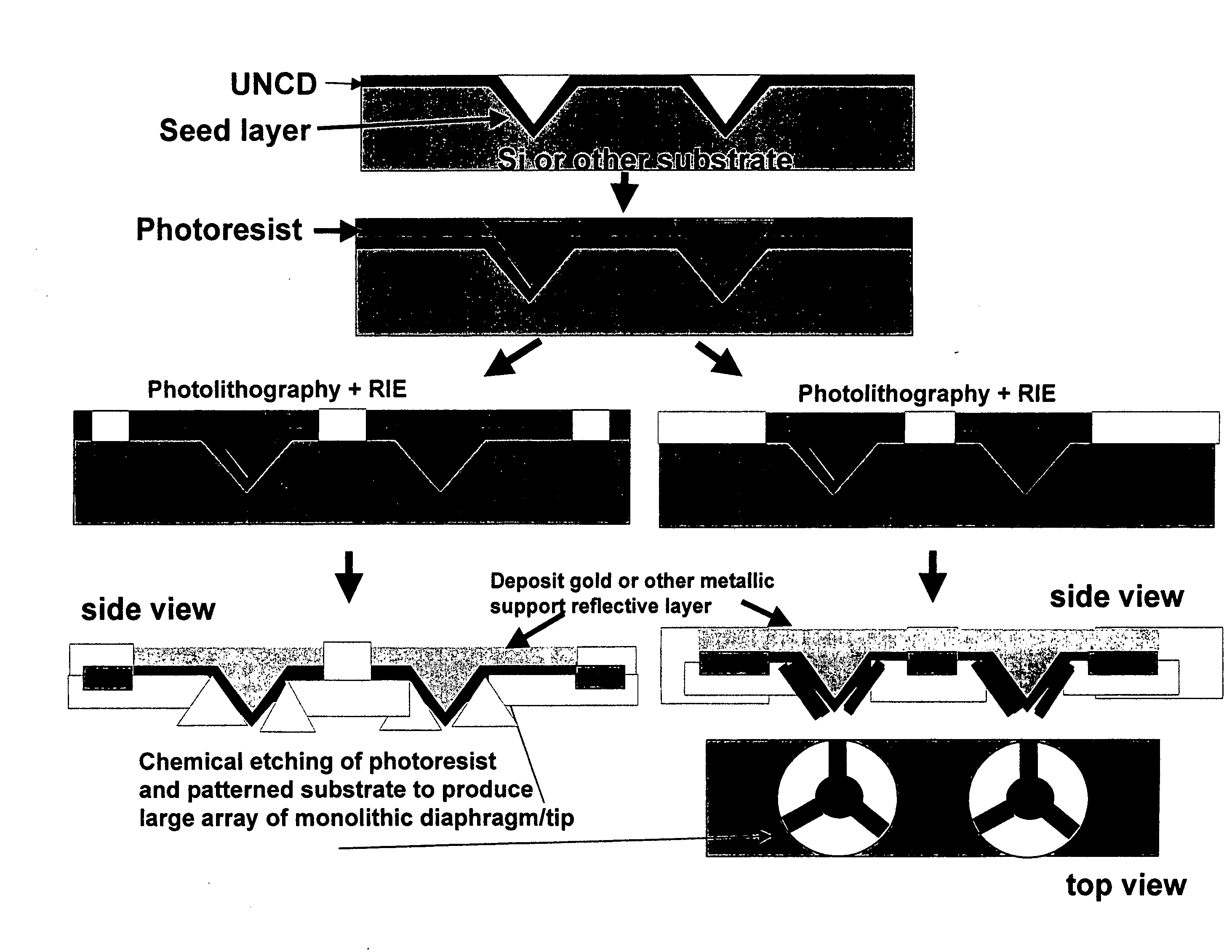
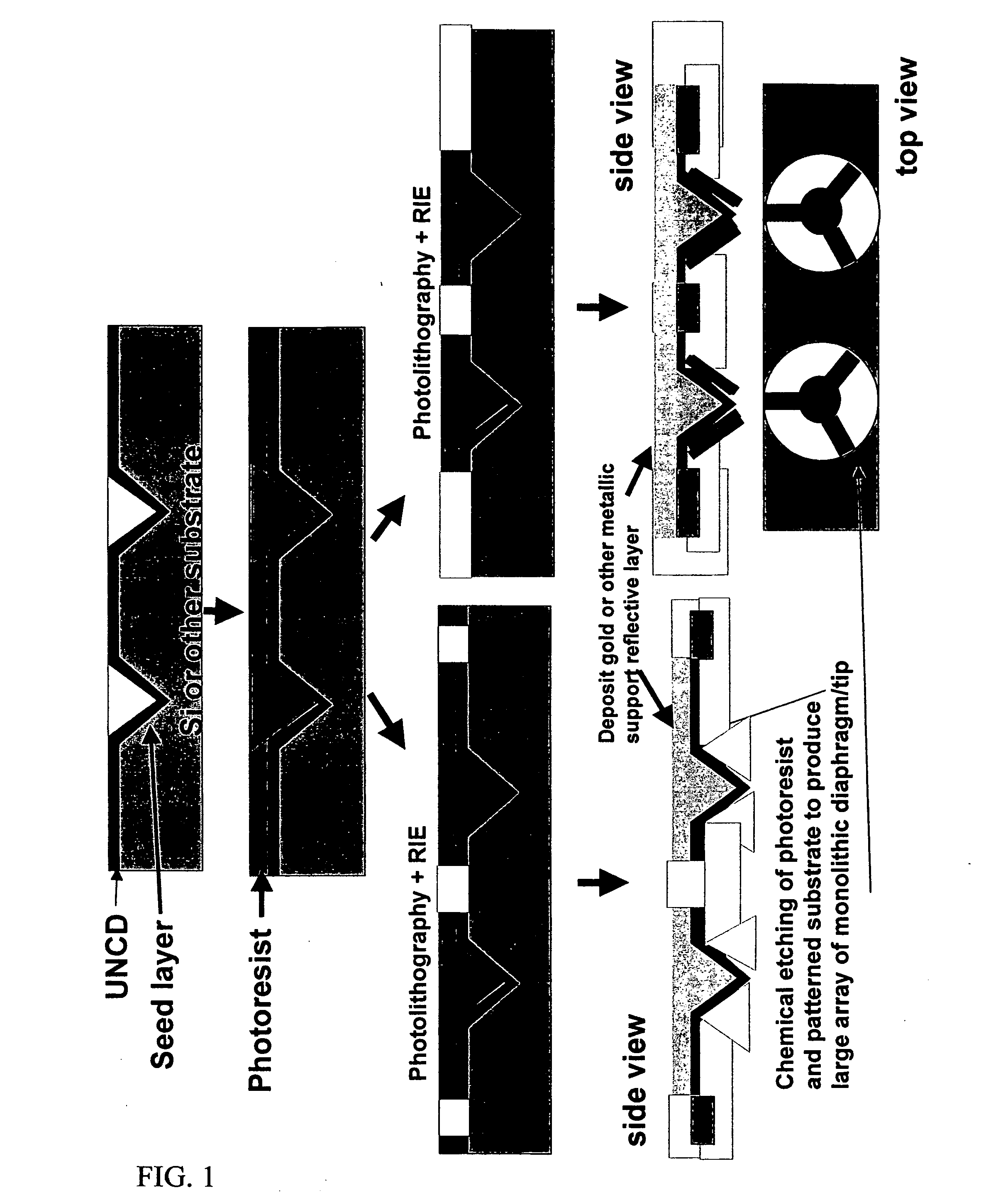
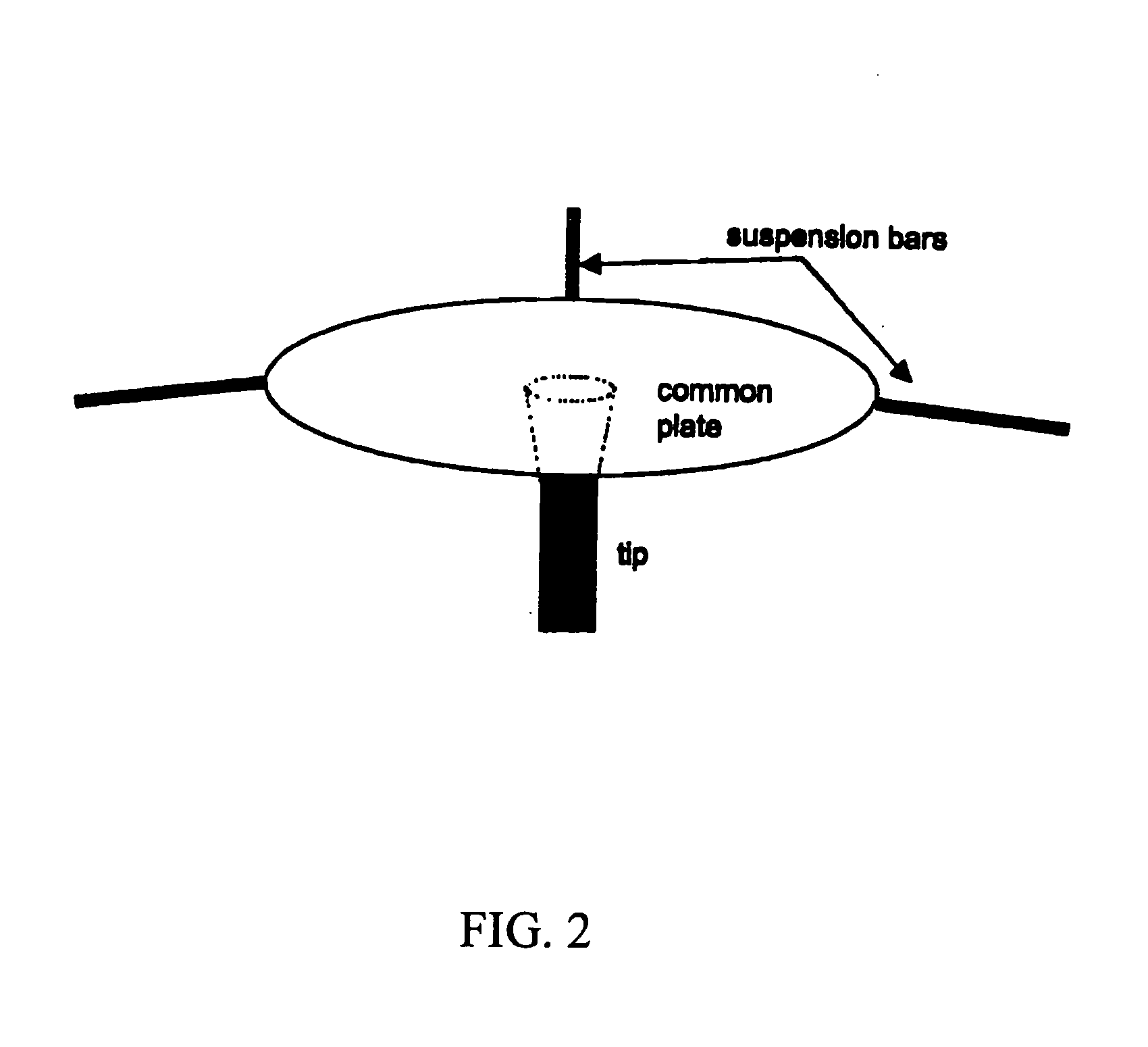
[0016]UNCD films, as discussed by R. Rameshan, Thin Solid Films 1999, 340, 1-6; T. A. Friedmann, J. P. Sullivan, J. A. Knapp, D. R. Tallant, D. M. Follstaedt, D. L. Medlin, P. B. Mirkarimi, Appl. Phys. Lett. 1997, 71, 3820-3822; A. R. Kraus, O. Auciello, D. M. Gruen, A. Jayatissa, A. Sumant, J. Tucek, D. C. Mancini, N. Moldovan, A. Erdemir, D. Ersoy, M. N. Gardos, H. G. Busmann, E. M. Meyer, M. Q. Ding, Diamond Relat. Mater. 2001, 10, 1952-1961; a) H. D. Espinosa, B. C. Prorok, B. Peng, K.-H. Kim, N. Moldovan, O. Auciello, J. A. Carlisle, D. M. Gruen, D. C. Mancini, Exp. Mech. 2003, 43, 256-268; b) H. D. Espinosa, B. Peng, B. C. Prorok, N. Moldovan, O. Auciello, J. A. Carlisle, D. M. Gruen, D. C. Mancini, J. Appl. Phys. 2003, 94, 6076-6084; and A. Erdemir, C. Bindal, G. R. Fenske, C. Zuiker, R. Csencsits, A. R. Krauss, D. M. Gruen, Diamond Relat. Mater. 1996, 6, 31-47, all incorporated herein by reference, with grain sizes in the 2-5 nm range, retain most of the surface and bulk pro...


PUM


Abstract

A monolithically integrated 3-D membrane or diaphragm / tip (called 3-D tip) of substantially all UNCD having a tip with a radius of about less than 50 nm capable of measuring forces in all three dimensions or being used as single tips or in large arrays for imprint of data on memory media, fabrication of nanodots of different materials on different substrates and many other uses such as nanolithography production of nanodots of biomaterials on substrates, etc. A method of molding UNCD is disclosed including providing a substrate with a predetermined pattern and depositing an oxide layer prior to depositing a carbide-forming metallic seed layer, followed by seeding with diamond nano or micropowder in solvent suspension, or mechanically polishing with diamond powder, or any other seeding method, followed by UNCD film growth conforming to the predetermined pattern. Thereafter, one or more steps of masking and / or etching and / or coating and / or selective removal and / or patterning and / or electroforming and / or lapping and / or polishing are used in any combination to form the tip or probe.

Description

RELATED APPLICATIONS[0001]This application is a continuation of application Ser. No. 11 / 388,636 filed Mar. 24, 2006.CONTRACTUAL ORIGIN OF THE INVENTION[0002]The United States Government has rights in this invention pursuant to Contract No. W-31-109-ENG-38 between the U.S. Department of Energy and UChicago Argonne LLC representing Argonne National Laboratory.FIELD OF THE INVENTION[0003]This invention relates to molding ultrananocrystalline diamond (UNCD) and particularly three dimensional probes used in atomic force microscopy (AFM).BACKGROUND OF THE INVENTION[0004]The sensing of small forces in a reliable and accurate manner is a key scientific and technological capability being harnessed across many scientific disciplines and in many industries. This is accomplished using atomic force microscopy (AFM) in applications such as topographic imaging, metrology, nanomachining, nanolithography, nanomanufacturing, nanoscale data storage, nanotribology measurements, and nanomechanical chara...

Claims


Application Information

Patent Timeline
Patent Type & Authority Applications(United States)
IPC IPC(8): G01B5/28
CPCB82Y35/00G01Q70/14G01Q60/38
Inventor SUMANT, ANIRUDHA V.CARPICK, ROBERT W.AUCIELLO, ORLANDO H.CARLISLE, JOHN A.
Owner UCHICAGO ARGONNE LLC
Why Eureka
Try Eureka