Nanowires comprising metal nanodots and method for producing the same

a technology of nanowires and metal nanodots, which is applied in the field of nanowires including metal nanodots, can solve the problems of difficult to form pores having a size, unsatisfactory mass production of nanowires, and limited template approaches

Inactive Publication Date: 2007-05-17
SAMSUNG ELECTRONICS CO LTD
View PDF3 Cites 21 Cited by
  • Summary
  • Abstract
  • Description
  • Claims
  • Application Information

AI Technical Summary

Problems solved by technology

However, since the template approach is a laboratory method and can be complicated and time-consuming to implement, it is not ideal for mass production of nanowires.
The diameter and length of the nanowires depend on the size and depth of the pores, and it can be very difficult to form pores having a size on the order of a few nanometers and a depth ranging from a few hundred micrometers to a few millimeters.
The

Method used


Image

  • Nanowires comprising metal nanodots and method for producing the same
  • Nanowires comprising metal nanodots and method for producing the same
  • Nanowires comprising metal nanodots and method for producing the same

Examples


example 1

Production of Silicon Nanowires

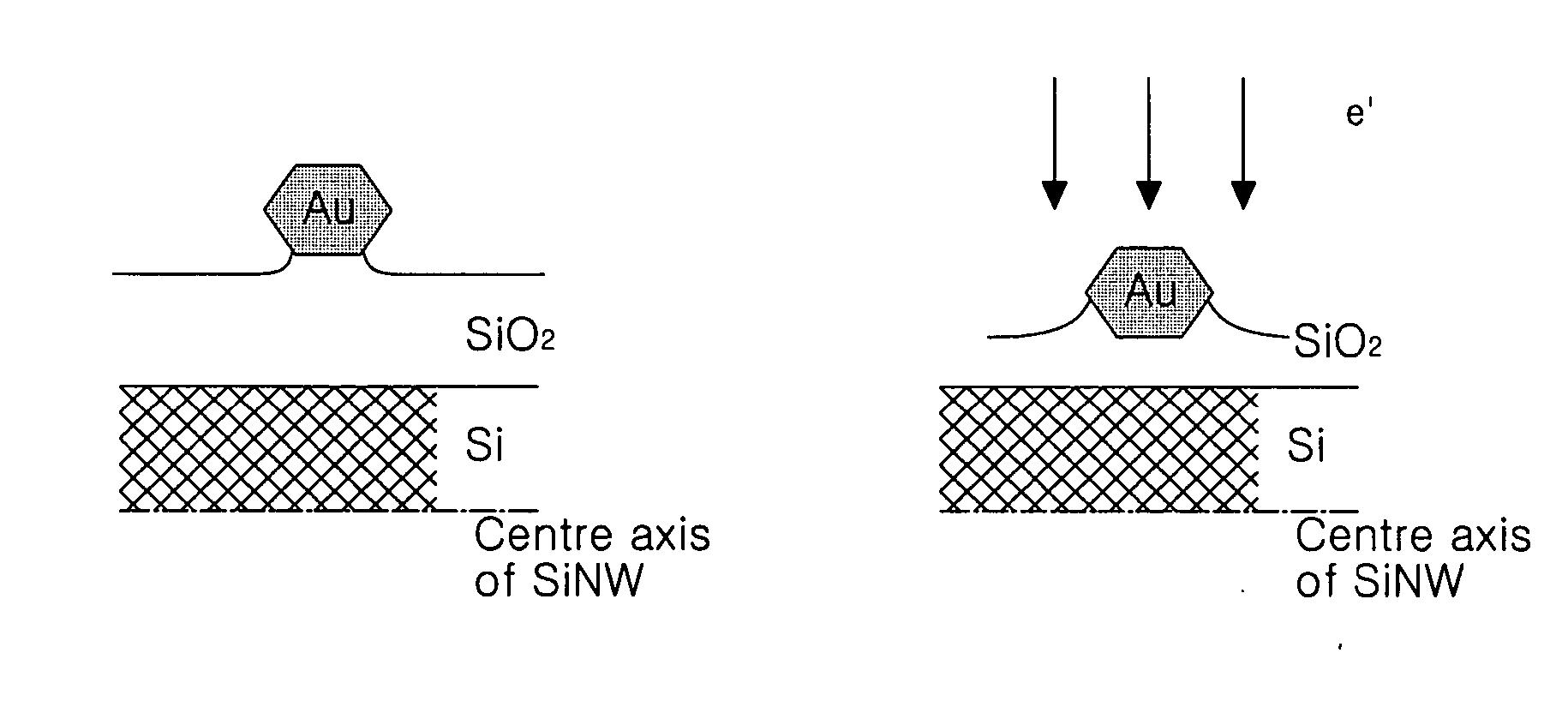
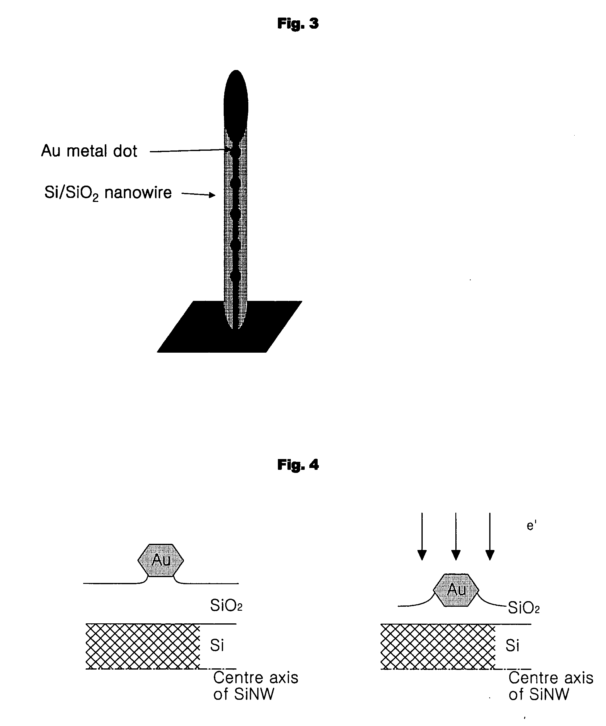
[0062] A natural oxide film was removed from a p-doped silicon substrate using an organic cleaning solvent or hydrofluoric acid. Gold (Au) nanoparticles (Nipponpaint Co., Ltd.) as catalyst particles were spin-coated onto the cleaned substrate to a thickness of about 30 nm. Subsequently, the coated substrate was placed in a reaction furnace, and the surface of the substrate onto which the nanowires would be grown was directed downward. The substrate was heated at a rate of about 10 to about 15° C. per minute, and maintained at a pressure of about 500 torr while argon (Ar) was fed into the furnace at a flow rate of about 100 sccm. The heated substrate was maintained at about 1000° C. for 30 minutes to grow the nanowires and metal nanodots. The resulting structure was slowly allowed to cool to about 700° C. under ambient conditions to complete the growth of the nanowires.

[0063] The structure of the nanowires was examined by transmission electron microsc...


PUM


Abstract

Nanowires methods for producing the nanowires are provided. The nanowires include a plurality of metal nanodots uniformly disposed therein, and a core portion, wherein each of the plurality of metal nanodots is coupled to the core portion. According to the method, metal nanodots can be uniformly disposed in the nanowires, and nanowires having various physical properties can be produced by controlling the size and interval of the nanodots. Therefore, the nanowires can be effectively used in a variety of applications, including electronic devices, such as field effect transistors (FETs), sensors, photodetectors, light emitting diodes (LEDs), and laser diodes (LDs).

Description

[0001] This application claims priority to Korean Patent Application No. 2005-106040 filed on Nov. 07, 2005 and to Korean Patent Application No. 2006-0004919 filed on Jan. 17, 2006 and all the benefits accruing therefrom under 35 U.S.C. § 119, the contents of which are herein incorporated by reference in their entireties. BACKGROUND OF THE INVENTION [0002] 1. Field of the Invention [0003] The present invention relates to nanowires including metal nanodots and a method for producing the nanowires. More particularly, the present invention relates to a new structure of nanowire including a plurality of metal nanodots uniformly disposed therein, and a method for producing the nanowires. [0004] 2. Description of the Related Art [0005] Nanowires are linear materials whose diameter is in the nanometer range (1 nm=10−9 m) and whose length is greater than the diameter. Nanowires can have a length on the order of several hundred nanometers, micrometers (1 μm=10−6 m), or millimeters (1 mm=10−3...

Claims


Application Information

Patent Timeline
IPC IPC(8): H01L21/44H01L23/52
CPCB82Y10/00H01L29/0665H01L29/0673H01L29/0676H01L33/18Y10S977/762Y10S977/70B82B3/00H01L21/20B82Y15/00
Inventor LEE, EUN KYUNGCHOI, BYOUNG LYONG
Owner SAMSUNG ELECTRONICS CO LTD
Why Eureka
Try Eureka