Enhancing performance in ink-jet printed organic semiconductors

a technology of organic semiconductors and ink-jet printing, applied in the direction of organic semiconductor devices, solid-state devices, material nanotechnology, etc., can solve the problems of slow circuits created using organic semiconductor processing technology, less durable circuits, etc., and achieve the effect of improving the performance of electronic and optoelectronic circuits

Inactive Publication Date: 2007-11-29
CUTS
View PDF10 Cites 23 Cited by
  • Summary
  • Abstract
  • Description
  • Claims
  • Application Information

AI Technical Summary

Benefits of technology

[0009]In accordance with the present invention, systems and methods are provided to improve the performance of electronic and optoelectronic circuits made using organic semiconductor processing technology.

Problems solved by technology

But circuits created using organic semiconductor processing technology are slower and less durable than circuits created using CMOS processing technology.

Method used


Image

  • Enhancing performance in ink-jet printed organic semiconductors
  • Enhancing performance in ink-jet printed organic semiconductors
  • Enhancing performance in ink-jet printed organic semiconductors

Examples


Embodiment Construction

[0023]In the following description, numerous specific details are set forth regarding the systems and methods of the present invention and the environment in which such systems and methods may operate, etc., in order to provide a thorough understanding of the present invention. It will be apparent to one skilled in the art, however, that the present invention may be practiced without such specific details, and that certain features, which are well known in the art, are not described in detail in order to avoid complication of the subject matter of the present invention. In addition, it will be understood that the examples provided below are exemplary, and that it is contemplated that there are other systems and methods that are within the scope of the present invention.

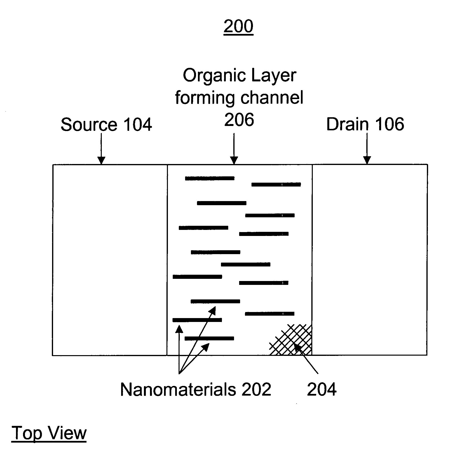
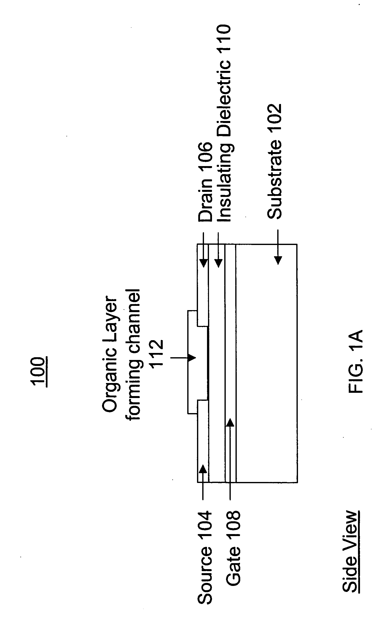
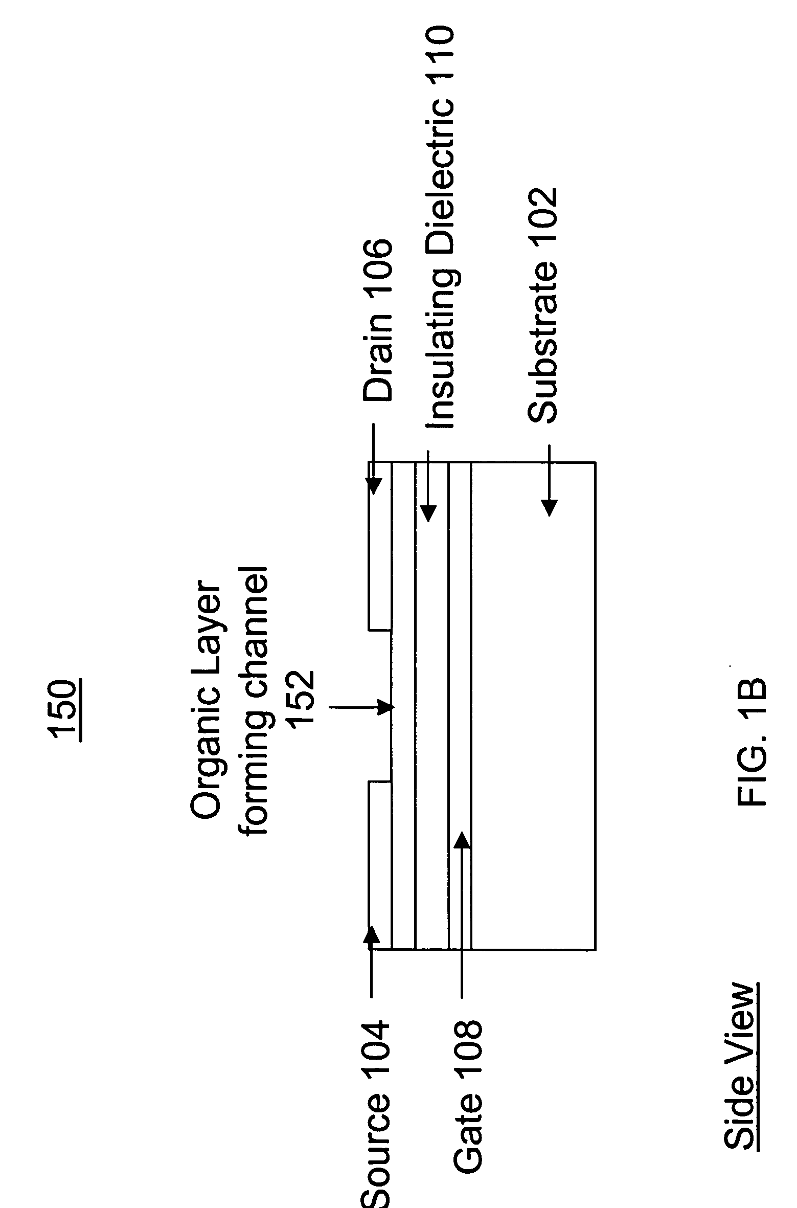
[0024]In accordance with the present invention, systems and methods are provided to improve the performance of electronic and optoelectronic circuits made using organic semiconductor processing technology. The electro...


PUM


Abstract

Systems and methods are provided to improve the performance of electronic and optoelectronic devices made using organic semiconductor processing technology. An ink-jet device dispenses an organic composite mixture onto a substrate. The mixture includes a semiconducting polymer and nanomaterials dispersed into an organic solvent. The type of solvent used preferably achieves effective dispersion of the polymer and nanomaterials in the solvent to minimize the occurrence of clogging of the ink-jet nozzles. The range of nanomaterials include, but are not limited to, organic and inorganic, single or multi-walled nanotubes, nanowires, nanodots, quantum dots, nanorods, nanocrystals, nanotetrapods, nanotripods, nanobipods, nanoparticles, nanosaws, nanosprings, nanoribbons, any branched nanostructure, and any mixture of these nanoshaped materials. The nanostructures can be aligned on the substrate to improve the carrier mobility in the organic semiconductors.

Description

[0001]This patent disclosure contains material that is subject to copyright protection. The copyright owner has no objection to the facsimile reproduction by anyone of the patent document or the patent disclosure as it appears in the U.S. Patent and Trademark Office patent file or records, but otherwise reserves any and all copyright rights.1. FIELD OF THE INVENTION[0002]The present invention relates to polymer-based electronic and optoelectronic devices fabricated by ink-jet printing techniques. More particularly, the present invention relates to using nanomaterials to improve the performance of ink-jet printed devices.2. BACKGROUND OF THE INVENTION[0003]Semiconductor technology has played an important role in the development of electronic circuits over the past several decades. Two examples of semiconductor technology include complementary metal oxide semiconductor (CMOS) processing technology and organic semiconductor processing technology.[0004]CMOS processing technology has bee...

Claims


Application Information

Patent Timeline
Patent Type & Authority Applications(United States)
IPC IPC(8): H01L51/40
CPCB82Y20/00B82Y30/00H01L51/0005Y02E10/549H01L51/5052H01L2251/5369H01L51/0545H10K71/135H10K10/466H10K2102/331
Inventor BEECHER, PAULCOLLI, ALANROZHIN, OLEKSLYSERVATI, PEYMANFASOLI, ANDREAFERRARI, ANDREA C.FLEWITT, ANDREWROBERTSON, JOHNMILNE, WILLIAM I.
Owner CUTS
Why Eureka
Try Eureka