Charge storage nodes with conductive nanodots

a technology of charge storage nodes and nanodots, which is applied in the field of memory cells with charge storage nodes, memory cells for nonvolatile memory devices, etc., can solve problems such as data retention, program saturation and trapping, and tend to worsen

Active Publication Date: 2011-07-28
MICRON TECH INC
View PDF7 Cites 21 Cited by
  • Summary
  • Abstract
  • Description
  • Claims
  • Application Information

AI Technical Summary

Problems solved by technology

As memory densities increase, issues with data re...

Method used


Image

  • Charge storage nodes with conductive nanodots
  • Charge storage nodes with conductive nanodots
  • Charge storage nodes with conductive nanodots

Examples


Embodiment Construction

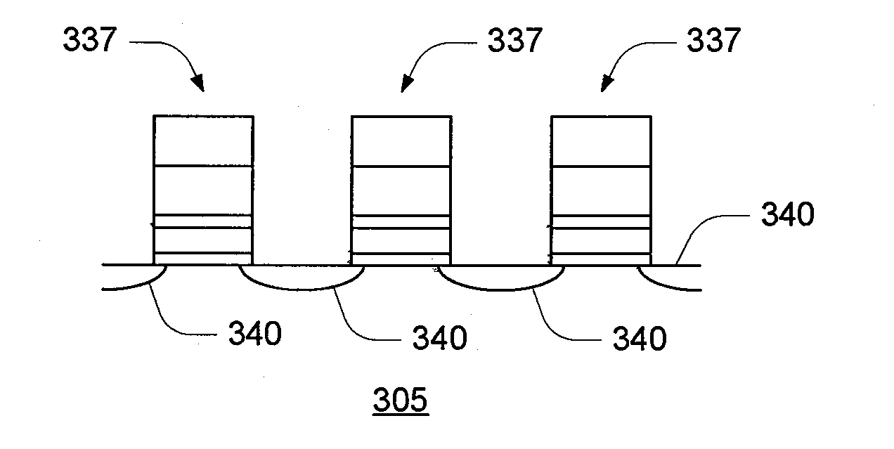
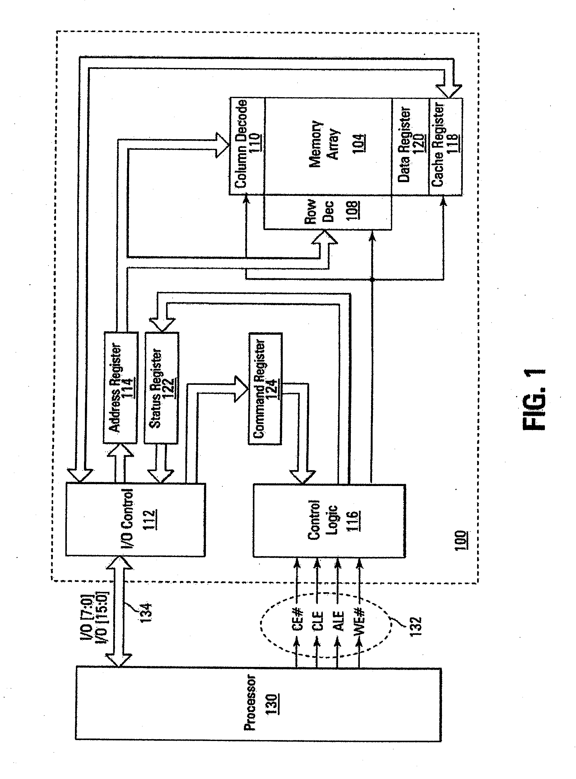
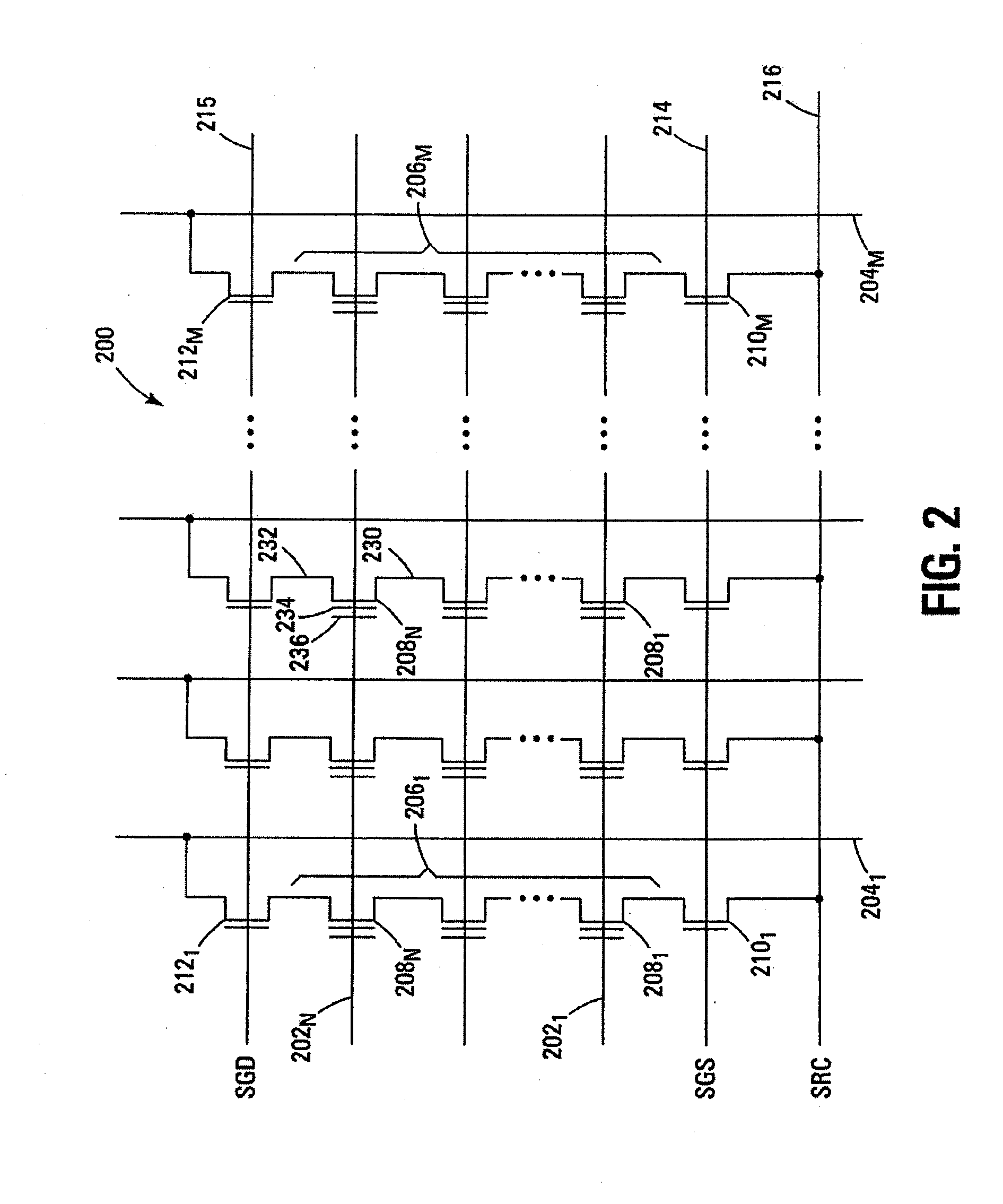
In the following detailed description, reference is made to the accompanying drawings that form a part hereof, and in which is shown, by way of illustration, specific embodiments. In the drawings, like numerals describe substantially similar components throughout the several views. Other embodiments may be utilized and structural, logical, and electrical changes may be made without departing from the scope of the present disclosure. The term semiconductor can refer to, for example, a layer of material, a wafer, or a substrate, and includes any base semiconductor structure. “Semiconductor” is to be understood as including silicon on sapphire (SOS) technology, silicon on insulator (SOI) technology, thin film transistor (TFT) technology, doped and undoped semiconductors, epitaxial layers of a silicon supported by a base semiconductor structure, as well as other semiconductor structures well known to one skilled in the art. Furthermore, when reference is made to a semiconductor in the f...


PUM


Abstract

Memory cells formed to include a charge storage node having conductive nanodots over a charge storage material are useful in non-volatile memory devices and electronic systems.

Description

TECHNICAL FIELD OF THE INVENTIONThe present disclosure relates generally to semiconductor memories and, in particular, in one or more embodiments, the present disclosure relates to memory cells for non-volatile memory devices, the memory cells having charge storage nodes.BACKGROUND OF THE INVENTIONMemory devices are typically provided as internal, semiconductor, integrated circuits in computers or other electronic devices. There are many different types of memory including random-access memory (RAM), read only memory (ROM), dynamic random access memory (DRAM), synchronous dynamic random access memory (SDRAM), and flash memory.Flash memory devices have developed into a popular source of non-volatile memory for a wide range of electronic applications. Flash memory devices typically use a one-transistor memory cell that allows for high memory densities, high reliability, and low power consumption. Changes in threshold voltage of the cells, through programming (which is sometimes referr...

Claims


Application Information

Patent Timeline
IPC IPC(8): H01L29/792H01L21/336
CPCB82Y10/00H01L27/11521H01L21/28273H01L29/7881H01L29/42332H01L29/40114Y10S977/774Y10S977/943H10B41/30H10B41/35H01L29/7883
Inventor RAMASWAMY, NIRMAL
Owner MICRON TECH INC
Why Eureka
Try Eureka