Apparatus and method for supplying slurry for a semiconductor

Inactive Publication Date: 2011-07-21
C&G HI TECH
View PDF79 Cites 4 Cited by
  • Summary
  • Abstract
  • Description
  • Claims
  • Application Information

AI Technical Summary

Benefits of technology

According to the present invention, unlike a conventional filter (unidirectional filter), the filter used in the present invention is automatically back-washed before being clogged with the slurry, and thus the filter can be used continuously for a long time period without cessation of the filtering process, thereby increasing the filtering efficiency.
Further, since the large-s

Problems solved by technology

In other words, there is a tendency that surface structure of a semiconductor device is further complicated, and also a step between interlayer films is further increased.
The step between interlayer films may cause a process error.
If large-sized particles (e.g., typically 1μ or more in case of oxide slurry) are used in the CMP process, fine patterns formed on the semiconductor waf

Method used


Image

  • Apparatus and method for supplying slurry for a semiconductor
  • Apparatus and method for supplying slurry for a semiconductor
  • Apparatus and method for supplying slurry for a semiconductor

Examples


Example

BEST MODE

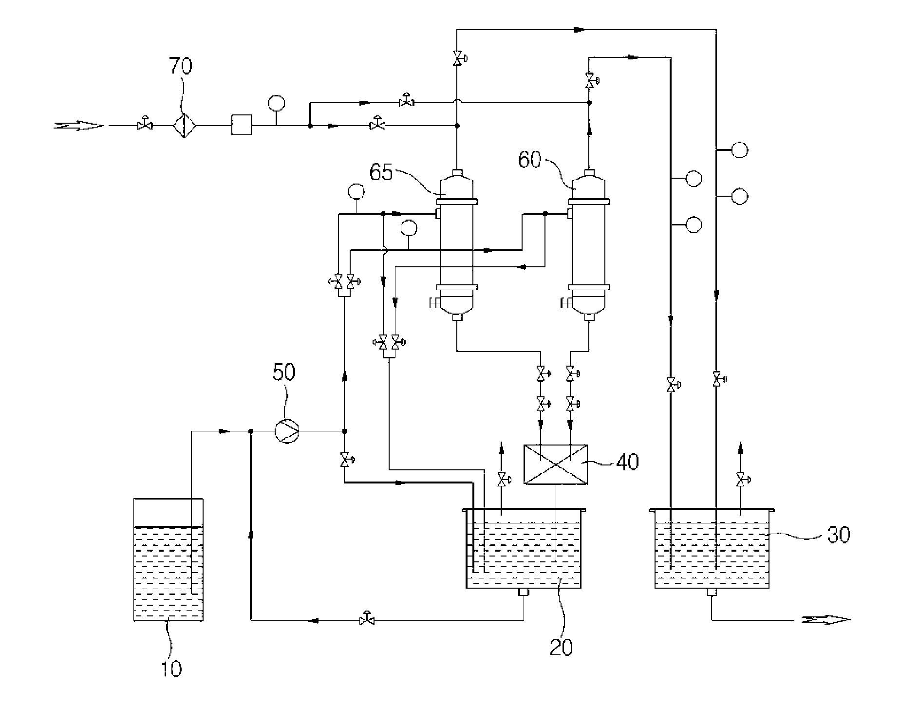
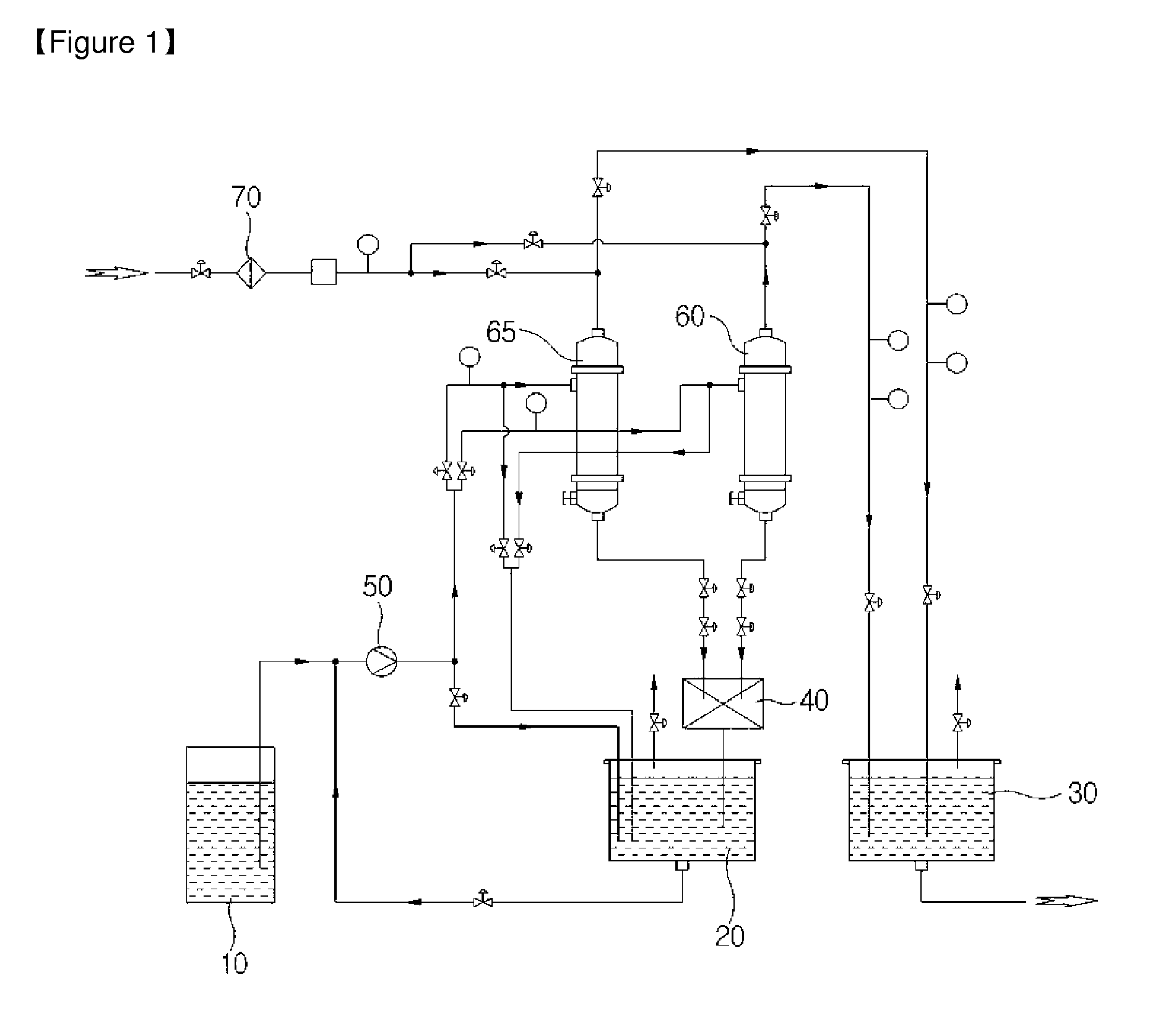
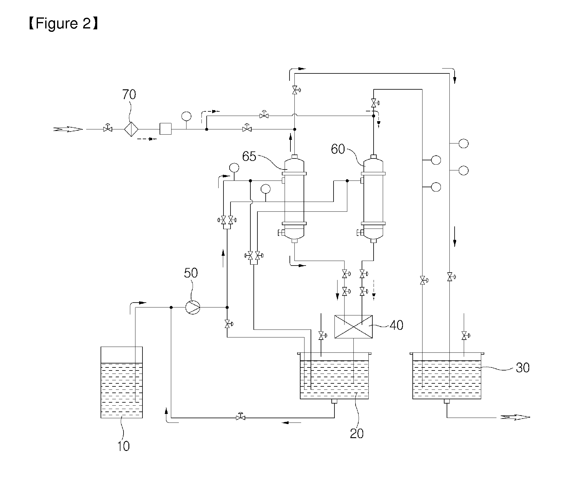
Hereinafter, the embodiments of the present invention will be described in detail with reference to accompanying drawings. FIG. 1 is a schematic view of an apparatus for supplying slurry for semiconductor according to the present invention and FIG. 2 is a view showing a process for backwashing one of filters in the apparatus for supplying slurry for semiconductor according to the present invention.

As shown in drawings, the apparatus for supplying slurry for semiconductor according to the present invention includes a slurry supplying tank 10, a filter 60, 65, a slurry collecting tank 20, an air injector 70 and a disintegrator 40.

Herein, slurry as an abrasive is supplied from the slurry supplying tank 10 and then collected in the slurry collecting tank 20. Further, the collected slurry is supplied to the filter 60, 65 by a pump 50 (or other pressing means) connected through a pipe line. Herein, the slurry may be directly supplied from the slurry supplying tank 10 to the filte...


PUM

PropertyMeasurementUnit
Particle sizeaaaaaaaaaa
Frequencyaaaaaaaaaa

Abstract

Disclosed is an apparatus for supplying slurry for semiconductor, including a filter which filters slurry particles larger than a predetermined particle size; an air injector which is connected with the filter so as to back-wash the filter using compressed air injected into the filter; a slurry collecting tank which is connected with the filter so as to store the slurry filtered by the filter; and a disintegrator which is connected with the slurry collecting tank so as to crush the filtered slurry.

Description

TECHNICAL FIELDThe present invention relates to an apparatus for supplying slurry for semiconductor and a method thereof, and particularly, to an apparatus for supplying slurry for semiconductor and a method thereof, which can use a whole amount of an abrasive for a CMP process without waste of a residual amount thereof.BACKGROUND ARTGenerally, in a process technology for manufacturing a semiconductor device, it is required to form finer patterns according to the requirement for high integration and high density.Thus, the requirement for multi-layer wiring structure is gradually increased in various fields. In other words, there is a tendency that surface structure of a semiconductor device is further complicated, and also a step between interlayer films is further increased. The step between interlayer films may cause a process error.To solve the problem, there has been various conventional methods of planarizing semiconductor wafers, such as SOG, Etch back BPSG (Boron Phosphorus S...

Claims


Application Information

Patent Timeline
IPC IPC(8): B01D24/46B01D35/00
CPCB24B57/02B24B37/04H01L21/304
Inventor KIM, HYUNG ILHONG, SA MUNKO, SE JONG
Owner C&G HI TECH
Why Eureka
Try Eureka