Information display device

a display device and information technology, applied in the direction of identification means, instruments, optics, etc., can solve the problems of large electric power consumption of the display device, achieve the effects of reducing the frame width, reducing the size, and improving the handling property

Inactive Publication Date: 2011-07-21
BRIDGESTONE CORP
View PDF1 Cites 22 Cited by
  • Summary
  • Abstract
  • Description
  • Claims
  • Application Information

AI Technical Summary

Benefits of technology

[0013]According to the present invention, electrical connection with an electronic component and a driving circuit provided on a rear surface of a substrate of an information display device is realized by a through-hole formed in the substrate, and unlike the conventional technique, it is not necessary to employ a TAB portion that externally protrudes from the substrate, whereby it is possible to achieve a display unit having reduced frame width as well as an information display device having reduced size. Further, since there does not exist any externally protruding portion such as the TAB portion, it is possible to improve a handling property at the time of an assembling process.

Problems solved by technology

However, in general, it has been known that the liquid display device consumes a large amount of electric power, and has various drawbacks such as a narrow viewing angle.

Method used


Image

  • Information display device
  • Information display device
  • Information display device

Examples


example 1

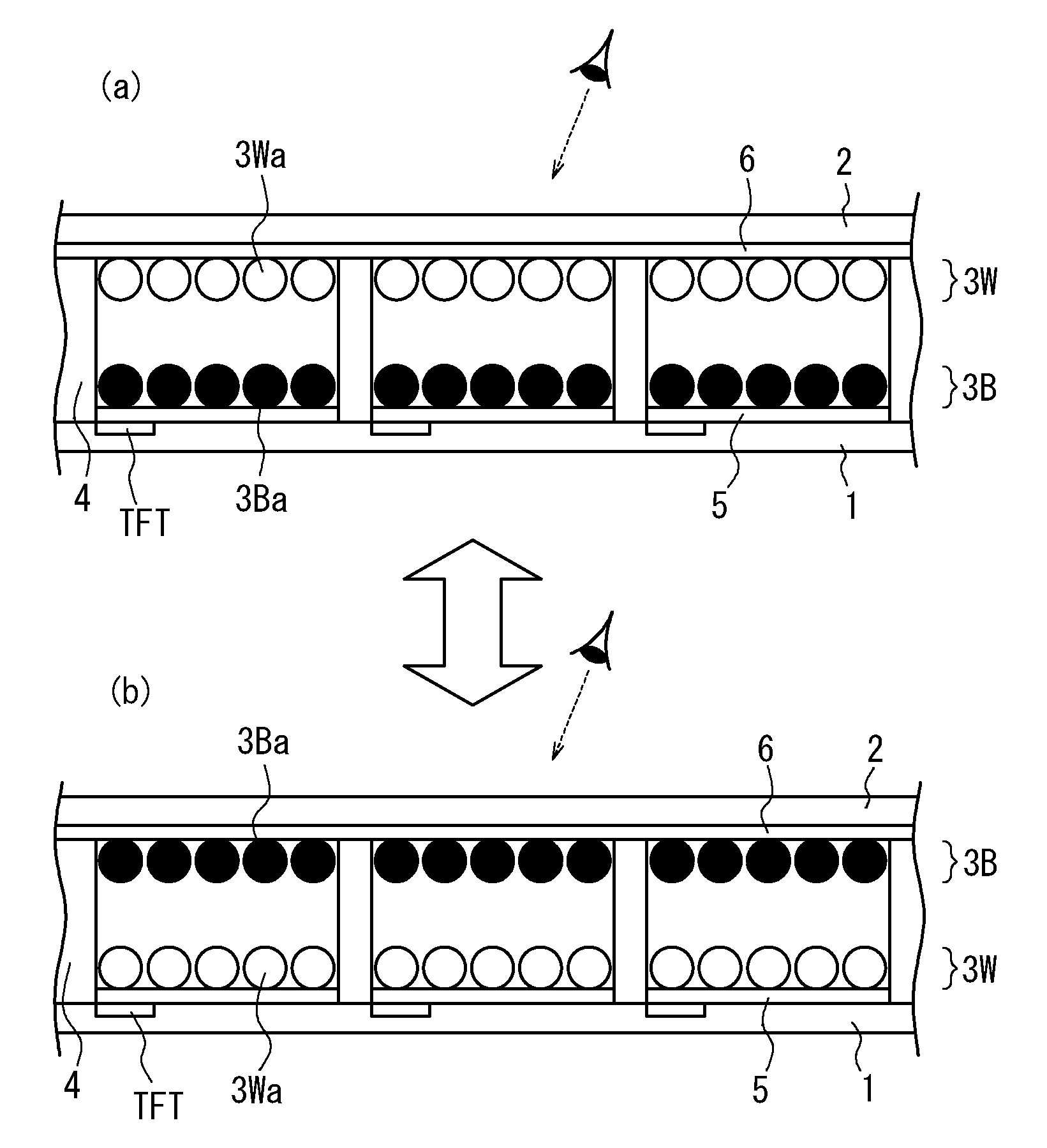
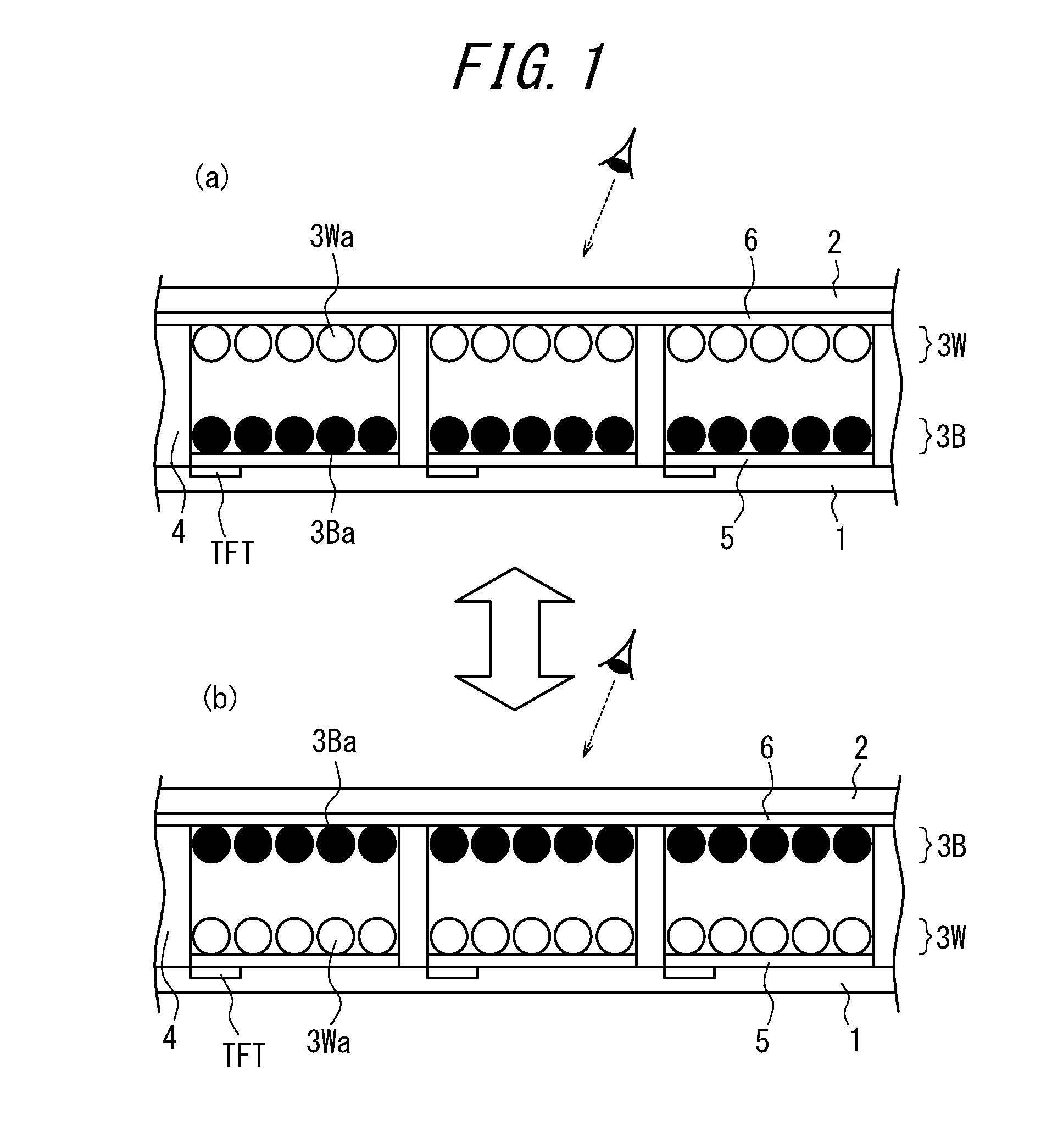
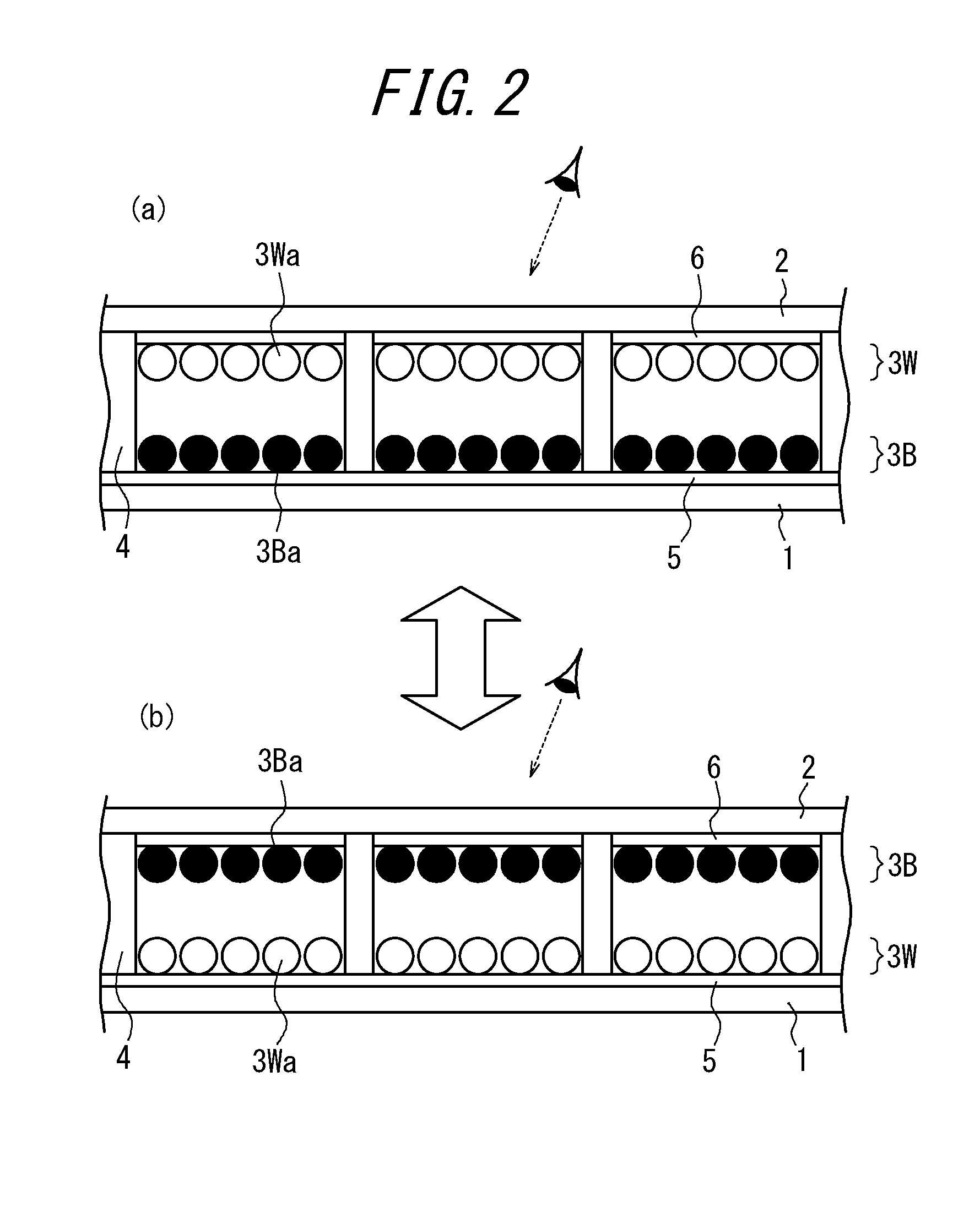
[0083]A back side substrate is prepared by: sputtering copper with a thickness of 1 μm on a polyethylene terephthalate (PET) film having a thickness of 100 μm to form a thin copper film; forming a line electrode on one side thereof, and a pad-like pattern for mounting on the other side thereof; forming a hole with a laser at a position where the line electrode and the pad for mounting (connection electrode) are connected, and applying a copper plating with a thickness of 1 μm so as not to protrude from the width of the electrode, to obtain a through-hole connection. As for a display side substrate, a display panel is prepared by using a substrate obtained by: sputtering an ITO film on a polyethylene terephthalate (PET) film having a thickness of 100 μm; and, forming a pattern of a line electrode.

example 1-1

[0084]In Example 1, both a width of the copper line electrode formed on the back side substrate and a width of a copper pad are set to 300 μm, and a hole having a diameter of 150 μm is formed with a laser.

example 1-2

[0085]In Example 1, both a width of the copper line electrode formed on the back side substrate and a width of a copper pad are set to 250 μm, and a hole having a diameter of 150 μm is formed with a laser.


PUM

PropertyMeasurementUnit
diameteraaaaaaaaaa
thicknessaaaaaaaaaa
thicknessaaaaaaaaaa

Abstract

An information display device, in which a display medium 3W, 3B having an optical reflectivity and comprised of a particle group containing particles that can be electrically driven is sealed between two panel substrates 5, 6 arranged so as to face each other, at least one of which panel substrates is transparent, and, the display medium is electrically moved via a pair of electrodes provided to the panel substrates and formed by the electrodes 5, 6, thereby to display information, in which the information display device has a structure in which a back side substrate 1, which is one of the two substrates, is connected with a wiring substrate 10; a first through-hole 7 penetrating the back side substrate for electrically connecting electrodes 5-1 and 5-2 provided on a front and a rear surfaces of the back side substrate is formed on the back side substrate, and the wiring substrate 10 is connected with the electrode 5-2 on the rear surface side within an area of the back side substrate; and, a second through-hole 7 for connecting an electrode 6 provided on a display side substrate, which is the other substrate of the two panel substrates, with the electrode 5-4 provided on the rear surface of the back side substrate is further formed.

Description

TECHNICAL FIELD[0001]The present invention relates to an information display device in which a display medium having an optical reflectivity and comprised of a particle group containing particles that can be electrically driven is sealed between two panel substrates arranged so as to face each other, at least one of which panel substrates is transparent, and, the display medium is electrically moved via a pair of electrodes provided to the panel substrates and forming a pixel, thereby to display information such as an image.RELATED ART[0002]As an information display device, a liquid crystal display device (LCD) is widely used. However, in general, it has been known that the liquid display device consumes a large amount of electric power, and has various drawbacks such as a narrow viewing angle. In view of the facts above, as a substitute for the liquid crystal display, there is proposed an information display device in which a display medium having an optical reflectivity and compri...

Claims


Application Information

Patent Timeline
Patent Type & Authority Applications(United States)
IPC IPC(8): G02F1/167G02F1/16755
CPCG02F1/1345G02F1/13452G09F9/00G02F2201/42G02F1/167G02F1/16755G02F1/1676G02F1/1681G02F2001/1678
Inventor SAKURAI, RYOOHNO, SHINGONISHIDA, MITSUHIROTANAKA, KANJINISHII, MASAYUKI
Owner BRIDGESTONE CORP
Why Eureka
Try Eureka