Thermal process

Inactive Publication Date: 2011-07-21
UNITED MICROELECTRONICS CORP
View PDF3 Cites 5 Cited by
  • Summary
  • Abstract
  • Description
  • Claims
  • Application Information

AI Technical Summary

Benefits of technology

[0009]According to a preferred embodiment of the present invention, a thermal process is disclosed. The thermal process preferably includes the steps of: providing a semiconductor substrate ready to be heated; and utilizing at least a first heating beam and a second heating beam with different energy density to heat the semiconductor substrate simultaneously. Accordingly, the present invention no only eliminates the need of switching between two different thermal processing equipments and shortens the overall fabrication cycle time, but also improves the patterning effect caused by the conventional front side heating substantially.

Problems solved by technology

Under this situation, many semiconductor fabrication processes face new challenges and bottlenecks, and therefore the manufacturers have to keep on researching new fabrication technologies to meet the request of high integration.
Nevertheless, the aforementioned rapid thermal processes, including the ones carried out with high temperature furnace or millisecond anneal process, still cause numerous problems.
The switch between equipments not only consumes a great deal of time, but also extends the cycle time of the overall fabrication.
However, when the surrounding of the semiconductor substrate of the transistor region is replaced by other non-silicon structure, such as shallow trench isolations (STIs) or other films are disposed on the semiconductor substrate, the thermal absorption capability of the doping regions is affected substantially during the thermal treatment process and results in a pattern effect.

Method used


Image

  • Thermal process
  • Thermal process
  • Thermal process

Examples


first embodiment

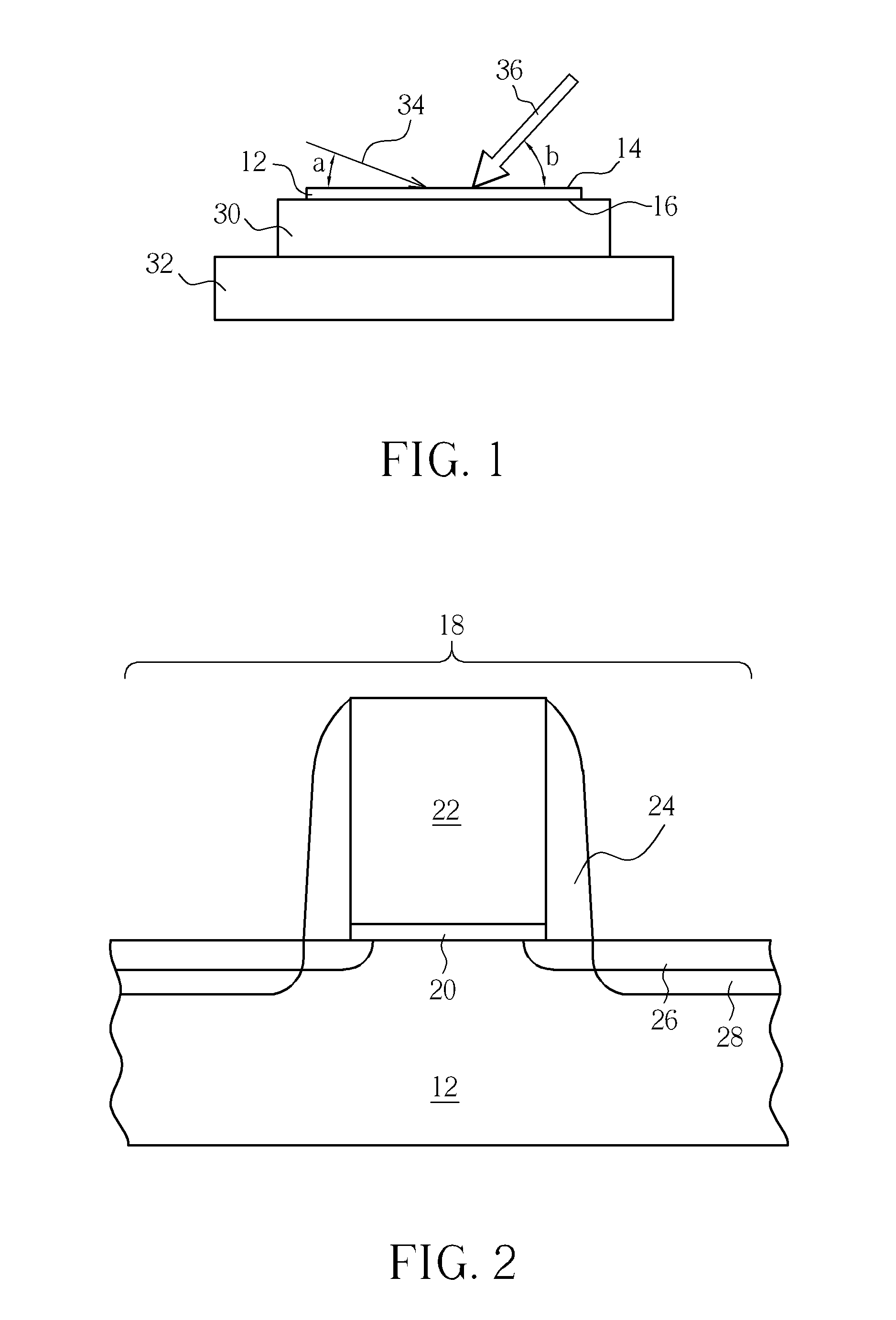
[0016]Referring to FIGS. 1-2, FIG. 1 illustrates a perspective view of performing a thermal process on a semiconductor substrate according to the present invention, and FIG. 2 illustrates a perspective view of a MOS transistor region of the semiconductor substrate. As shown in the figures, a semiconductor substrate 12, such as a silicon wafer ready to be heated is provided. The semiconductor substrate 12 has a front surface 14 and a back surface 16, in which a MOS transistor region 18 is defined on the front surface 14. Structures including a gate dielectric layer 20, a gate 22, and a spacer 24 are preferably formed on the front surface 14 of the semiconductor substrate 12. Moreover, at least one ion implantation is conducted to form a source / drain extension doping region (not shown) adjacent to two sides of the gate 22 in the semiconductor substrate 12 or a source / drain doping region (not shown) adjacent to two sides of the spacer 24 in the semiconductor substrate 12.

[0017]The semi...

second embodiment

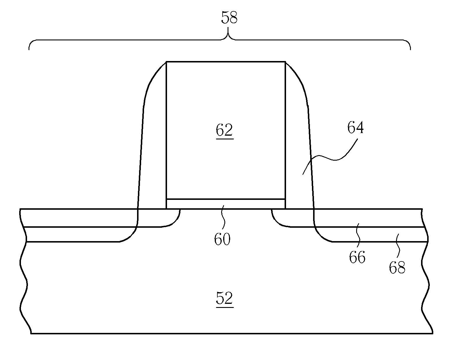
[0022]Referring to FIGS. 4-5, FIG. 4 illustrates a perspective view of performing a thermal process on a semiconductor substrate 52 according to the present invention, and FIG. 5 illustrates a perspective view of a MOS transistor region of the semiconductor substrate 52. As shown in the figures, a semiconductor substrate 52, such as a silicon wafer ready to be heated is provided. The semiconductor substrate 52 has a front surface 54 and a back surface 56, in which a MOS transistor region 58 is defined on the front surface 54. Structures including a gate dielectric layer 60, a gate 62, and a spacer 64 are preferably formed on the front surface 54 of the semiconductor substrate 52. Moreover, at least one ion implantation is conducted to form a source / drain extension doping region (not shown) adjacent to two sides of the gate 62 in the semiconductor substrate 52 or a source / drain doping region (not shown) adjacent to two sides of the spacer 64 in the semiconductor substrate 52.

[0023]Th...


PUM


Abstract

A thermal process is disclosed. The thermal process preferably includes the steps of: providing a semiconductor substrate ready to be heated; and utilizing at least a first heating beam and a second heating beam with different energy density to heat the semiconductor substrate simultaneously. Accordingly, the present invention no only eliminates the need of switching between two different thermal processing equipments and shortens the overall fabrication cycle time, but also improves the pattern effect caused by the conventional front side heating.

Description

BACKGROUND OF THE INVENTION[0001]1. Field of the Invention[0002]The invention relates to a thermal process, and more particularly, to a thermal process of using at least two heating beams with different energy density to heat a semiconductor substrate simultaneously.[0003]2. Description of the Prior Art[0004]With the advancing technology of the semiconductor industry, integrated circuits (ICs) are being developed to increase the current computing and storage capability, which pushes the development of related manufacturers forward. As predicted by Moore's law, the number of transistors doubles every 18 months. The process of semiconductor evolves from 0.18 nm of 1999, 0.13 μm of 2001, 90 nm of 2003 to 65 nm of 2005 and is approaching 45 nm. Therefore, the density of semiconductor elements on a wafer is increasing with the technology advancement of the semiconductor industry and miniaturization of microelectronic elements and makes the intervals between elements shorter and shorter. ...

Claims


Application Information

Patent Timeline
IPC IPC(8): H01L21/336H01L21/26
CPCH01L21/268H01L29/7833H01L29/6659
Inventor YANG, CHAN-LONLI, CHING-IKUO, TZU-FENG
Owner UNITED MICROELECTRONICS CORP
Why Eureka
Try Eureka