Processor circuit with shared memory and buffer system

a technology of processor circuit and buffer system, which is applied in the direction of electric digital data processing, instruments, sustainable buildings, etc., can solve the problems of inflexible use of architecture with two separate memory units, increased cost of alteration, and time-consuming and laborious alteration, so as to save space, save time when successive data is read, and reduce the surface area

Active Publication Date: 2011-07-28
EM MICROELECTRONIC-MARIN
View PDF5 Cites 5 Cited by
  • Summary
  • Abstract
  • Description
  • Claims
  • Application Information

AI Technical Summary

Benefits of technology

[0011]One advantage of the processor circuit is the possibility of saving time when successive data is read. Indeed, the management means for managing communications between the shared memory unit and the calculation unit are capable of saving the entire read memory section. This capacity allows the data of said saved section to be read directly from the management means if the other data stored in the section has to be read during the next read operation.
[0012]A second advantage of the processor circuit according to the invention is that it has a smaller surface area than that of a Harvard architecture according to the prior art. The use of a shared memory allows the processor circuit according to this invention to have only one physical memory to contain both data and instructions, thereby saving space. Thus for the same storage volume, a shared memory has a smaller surface area than two distinct memory units. This difference in surface area is due to the fact that, for the two distinct memory units, everything is doubled, such as the monitoring and control members, whereas for a shared memory, i.e. a single memory unit there is only one of each of these elements.
[0013]Another advantage is the flexibility of use of the shared memory. The fact of having a single memory unit allows more flexibility in the allocation of memory volume. This flexibility is a consequence of grouping data and instructions within the same physical unit. A virtual separation can easily be made and adapted to allocate more or less memory volume to data or instructions.

Problems solved by technology

However, this type of architecture has some drawbacks.
Moreover, this type of architecture with two separate memory units is not flexible to use.
This alteration involves additional costs due to the need to perform design work on the actual component.
However, this processor circuit still has two distinct memory units with a large surface area which does not resolve the surface area problem of the Harvard architecture.
Moreover, another drawback of this processor circuit is that it has flexibility of use resulting from a modification of the conventional Harvard architecture.
Thus, the flexibility provided by the processor circuit requires a profound alteration to the processor circuit and thus involves non negligible development costs.
Further, one of the drawbacks of storing data in the programme memory arises from the difference in size between data and instructions.
Thus when data stored in the instruction memory is read, only one part of the section is read which wastes time if successive data is read.

Method used


Image

  • Processor circuit with shared memory and buffer system
  • Processor circuit with shared memory and buffer system
  • Processor circuit with shared memory and buffer system

Examples


Embodiment Construction

[0018]In the following description, all those parts of the processor circuit which are well known to those skilled in the art in this technical field are only explained in a simplified manner.

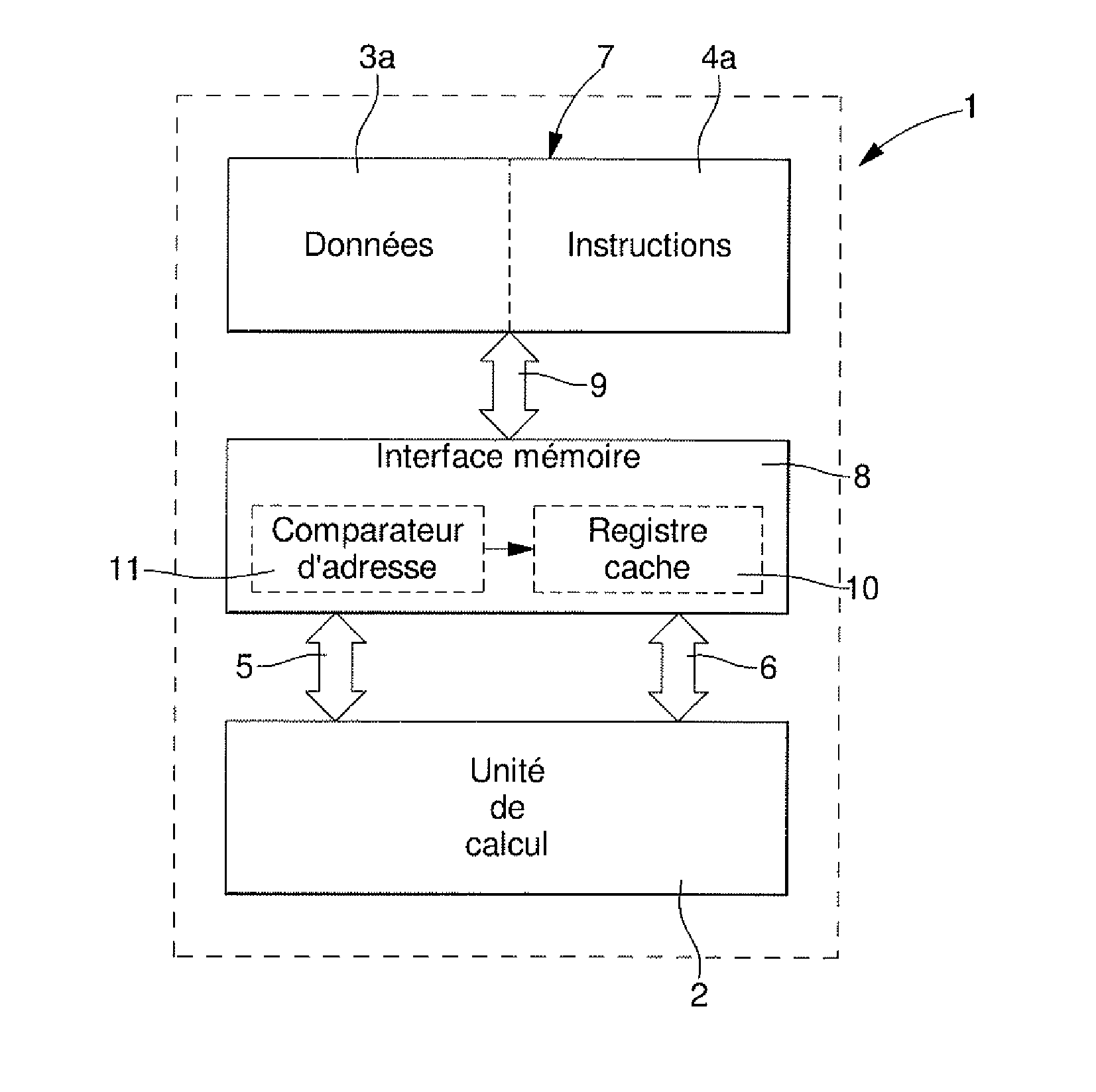
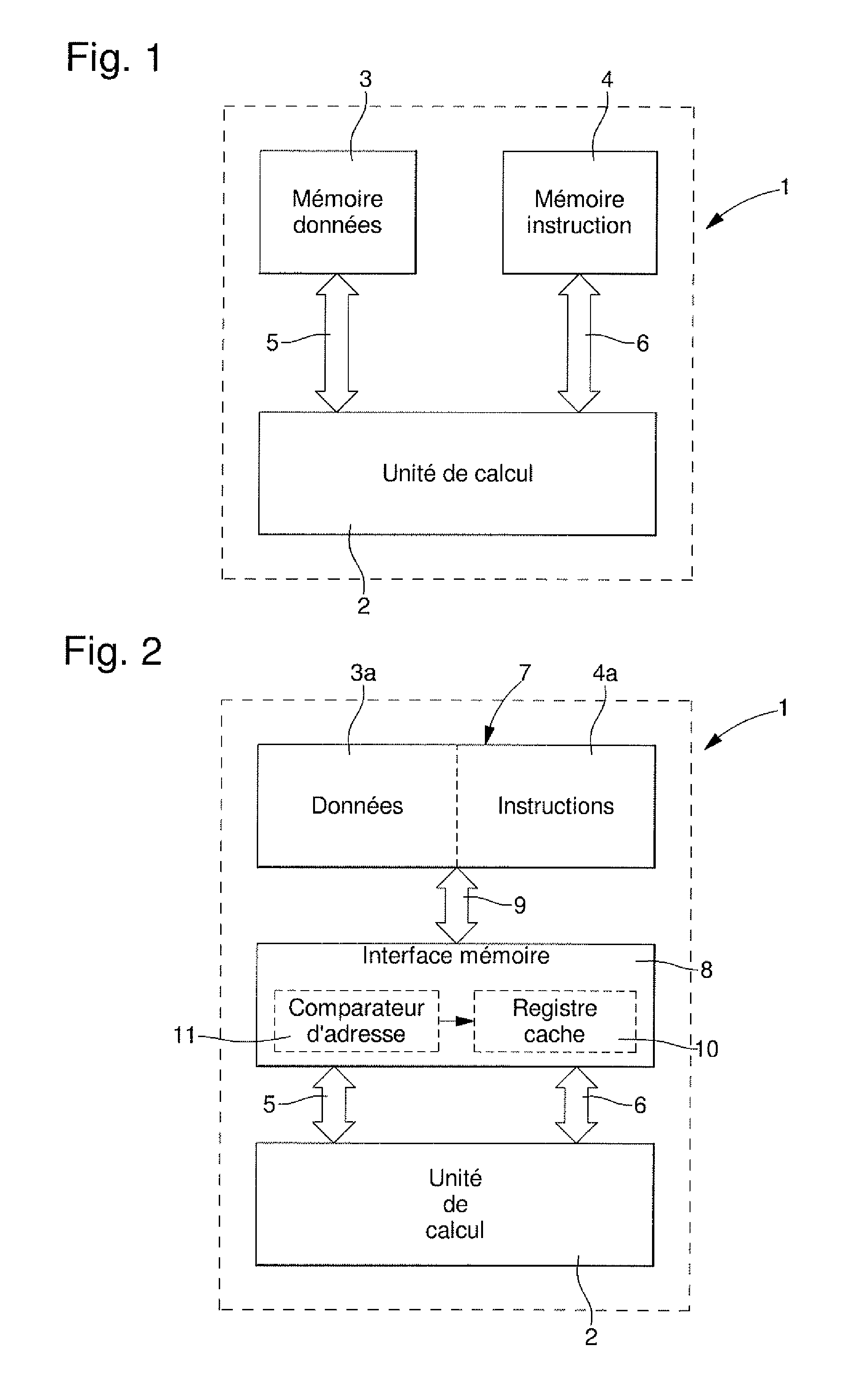
[0019]FIG. 2 shows schematically a processor circuit 1 having a Harvard architecture in accordance with this invention. This processor circuit 1 thus includes a calculation unit 2 and two memory elements 3a and 4a; one 3a containing data and the other, 4a, instructions. Calculation unit 2, also called an arithmetic and logic unit, is used for carrying out the basic operations, said unit 2 being the core of said processor unit. Calculation unit 2 communicates with memory elements 3a, 4a via respective communication buses 5, 6. These communication buses 5, 6 respectively connect said calculation unit 2 to memory element 3a containing data, and said calculation unit 2 to memory element 4a containing instructions and are respectively called the data bus 5 and programme bus 6. Communication means 5,...


PUM


Abstract

The processor circuit (1) has a Harvard architecture. This processor circuit includes a calculation unit (2), a first memory element (3a) for data storage and a second memory element (4a) for instruction storage. Said first and second memory elements (3a, 4a) are connected by at least one communication bus (5, 6) to the calculation unit. The processor circuit includes management means (8), placed between the first and second memory elements and the calculation unit and capable of saving several data items or instructions to save time during successive data reading.

Description

[0001]The present invention generally concerns a processor circuit. This processor circuit includes a calculation unit, a first memory element for data storage and a second memory element for instruction storage. Said first and second memory elements are connected by at least one communication bus to the calculation unit.BACKGROUND OF THE INVENTION[0002]Harvard type processor circuits are known in the prior art and are shown in FIG. 1. This Harvard architecture allows the processor circuit increased rapidity because instructions and data can be accessed at the same time. Processor circuits 1 having this architecture take the form of a calculation unit 2 communicating with two distinct memory units 3, 4. The first of the memory units 4 is used for storing instructions, while the second memory unit 3 is used for data storage. Each memory unit 3, 4 communicates with calculation unit 2 via a respective communication bus 5, 6. This architecture is thus characterized by the separation of ...

Claims


Application Information

Patent Timeline
Patent Type & Authority Applications(United States)
IPC IPC(8): G06F12/08G06F12/00G06F12/0897
CPCG06F12/0897Y02B60/1225G06F2212/1044G06F2212/1016Y02D10/00
Inventor THEODULOZ, YVESJAEGGI, HUGOTOTH, TOMAS
Owner EM MICROELECTRONIC-MARIN
Why Eureka
Try Eureka