OLED device and an electronic circuit

a technology of electronic circuits and diodes, which is applied in semiconductor devices, instruments, computing, etc., can solve the problems of difficult to determine the proper change in capacitance that will work for all conditions, and achieve the effects of reducing capacitance, reducing the thickness of the substrate, and reducing the capacitan

Inactive Publication Date: 2011-08-04
OLEDWORKS GMBH
View PDF15 Cites 7 Cited by
  • Summary
  • Abstract
  • Description
  • Claims
  • Application Information

AI Technical Summary

Benefits of technology

[0020]In another embodiment, the second substrate is constructed from a flexible material. This had the advantage that a touch sensor constructed out of a flexible material such as plastic can be mounted to the OLED means.
[0021]In another embodiment, embodiments of the invention provide for an OLED device where the thickness of the second substrate is chosen so that the capacitance between the OLED means and the two or more conductive elements is minimized. This is an advantage, because the change in capacitance when a finger is brought near to the NFI sensor is small in comparison to the capacitance between the two or more conductive elements and the OLED means. Increasing the thickness of the substrate reduces the capacitance and therefore makes it easier to detect the change in capacitance when someone touches the NFI screen.
[0022]In another embodiment the invention provides for an OLED device where the thickness of the first substrate is chosen so that the capacitance between the OLED means and the two or more conductive elements is minimized. This is an advantage, because the change in capacitance when a finger is brought near to the NFI sensor is small in comparison to the capacitance between the two or more conductive elements and the OLED means. Increasing the thickness of the substrate reduces the capacitance and therefore makes it easier to detect the change in capacitance when someone touches the NFI screen.
[0023]In another embodiment the two or more conductive elements are adapted for transmitting light. This is an advantage because the two or more conductive elements are positioned on the substrate where the light comes through the OLED means. If they are not adapted for transmitting light, it will reduce the amount of visible light which an operator or user is able to see. By making them transparent the device is more efficient. Conductive oxides such as ITO can be used to implement this. The conductive elements can also be adapted to transmit light by positioning the conductive elements so that they do not obstruct the light coming from the OLED means. Another alternative is to pattern the conductive elements such that the eye does not detect a regular pattern. This has the advantage of being less distracting to a user and making it less noticeable that there are conductive elements.
[0024]In another aspect the invention provides for an OLED apparatus comprised of the OLED device and an electronic circuit for powering and operating the OLED device. The electronic circuit is operable to calculate two or more capacitive coefficients of the capacitance formed by the two or more conductive elements for detecting a user input action. An advantage is that the calculation of these capacitances can be used to implement an NFI sensor, the advantages of which have already been discussed. Examples of user input actions are a user touching the surface to activate a switch, a user sliding his or her finger along the surface of the OLED device, or moving a finger in a circular motion on the surface of the OLED device. NFI sensors are able to detect the proximity of both conductive and dielectric objects. As a result a user input action can also be caused by moving an object into the proximity of the OLED device, or moving the object while it is in the proximity of the OLED device. This apparatus has the advantage that the OLED device is interfaced with the electronic circuit so that the OLED means is able to generate light, and the two or more conductive elements are connected to the electronic circuit which is able to detect if a touch has occurred and send a signal to another electronic circuit. This is useful because OLED apparatus is able to generate light and also to detect when an operator has touched it. This can be used for displays and control panels.
[0025]In another embodiment the electronic circuit is comprised of a means for providing the OLED means with a voltage bias, and a current generating means for generating a current flow in each of the two or more conductive elements. Providing the OLED means with a voltage bias is advantageous, because the OLED means requires a voltage bias to generate light. Generating a current flow in the two or more conductive elements is advantageous, because objects in proximity to the conductive elements change the conductive elements capacitance. This can be sensed and used to implement a capacitive proximity sensor. It is further comprised of a means for calculating two or more capacitive coefficients by either measuring the current flow through each of the conductive elements or by measuring the voltage drop across each of the conductive elements. If a known RF current is flowing through a conductive element, then a measurement of the RF voltage can be used to calculate the capacitance. If a known RF voltage is applied to a conductive element, then a measurement of the RF current can be used to calculate the capacitance. This is advantageous, because the two or more conductive elements can be used to implement an NFI type sensor. The advantages of which have already been explained. The circuit is also comprised of a signal generating means for generating a signal, were the signal depends upon the value of the two or more capacitive coefficients. One implementation is that the electronic circuit is incorporated into or interfaced with a second electronic circuit. This signal can also be implemented by the transmission of an analog or digital signal to another electronic circuit. This has the advantage that the OLED apparatus can be incorporated into a wide variety of control circuits.

Problems solved by technology

However, environmental conditions (e.g. the humidity) can affect the capacitance of the electrode to ground and make it difficult to determine the proper change in capacitance that will work for all conditions.

Method used


Image

  • OLED device and an electronic circuit
  • OLED device and an electronic circuit
  • OLED device and an electronic circuit

Examples


Embodiment Construction

[0034]Like numbered elements in these figures are either identical elements or perform the same function. Elements which have been discussed previously will not necessarily be discussed in later figures if the function is identical.

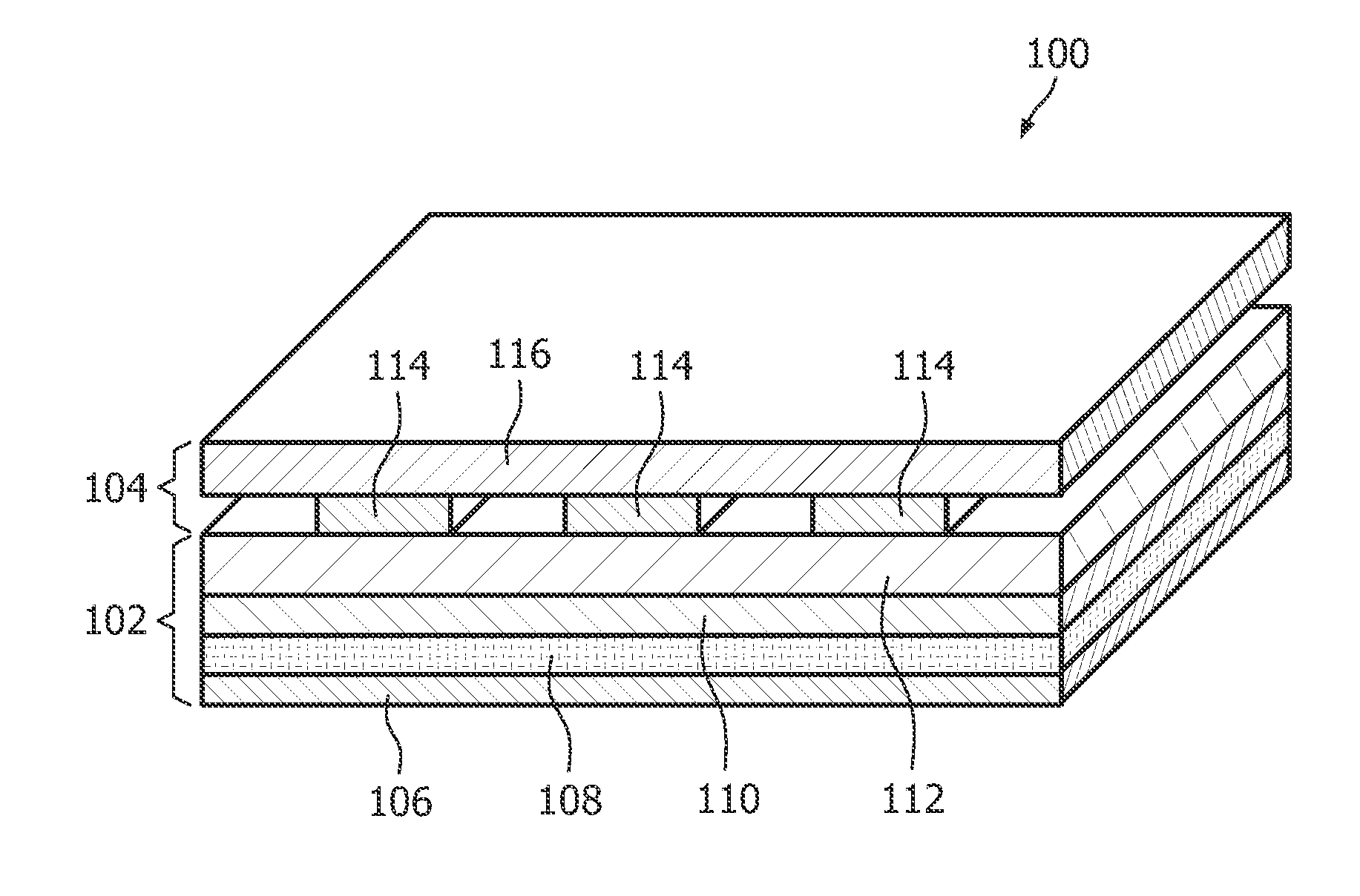
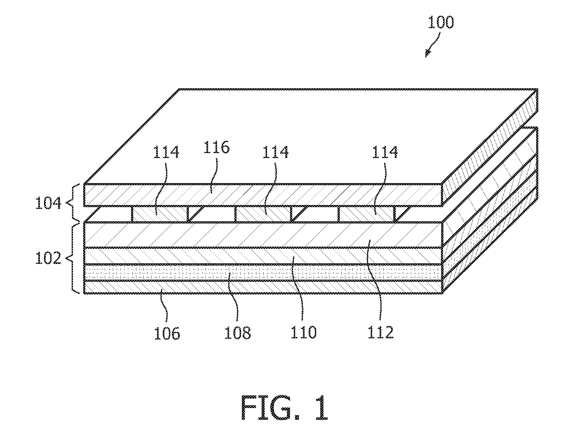
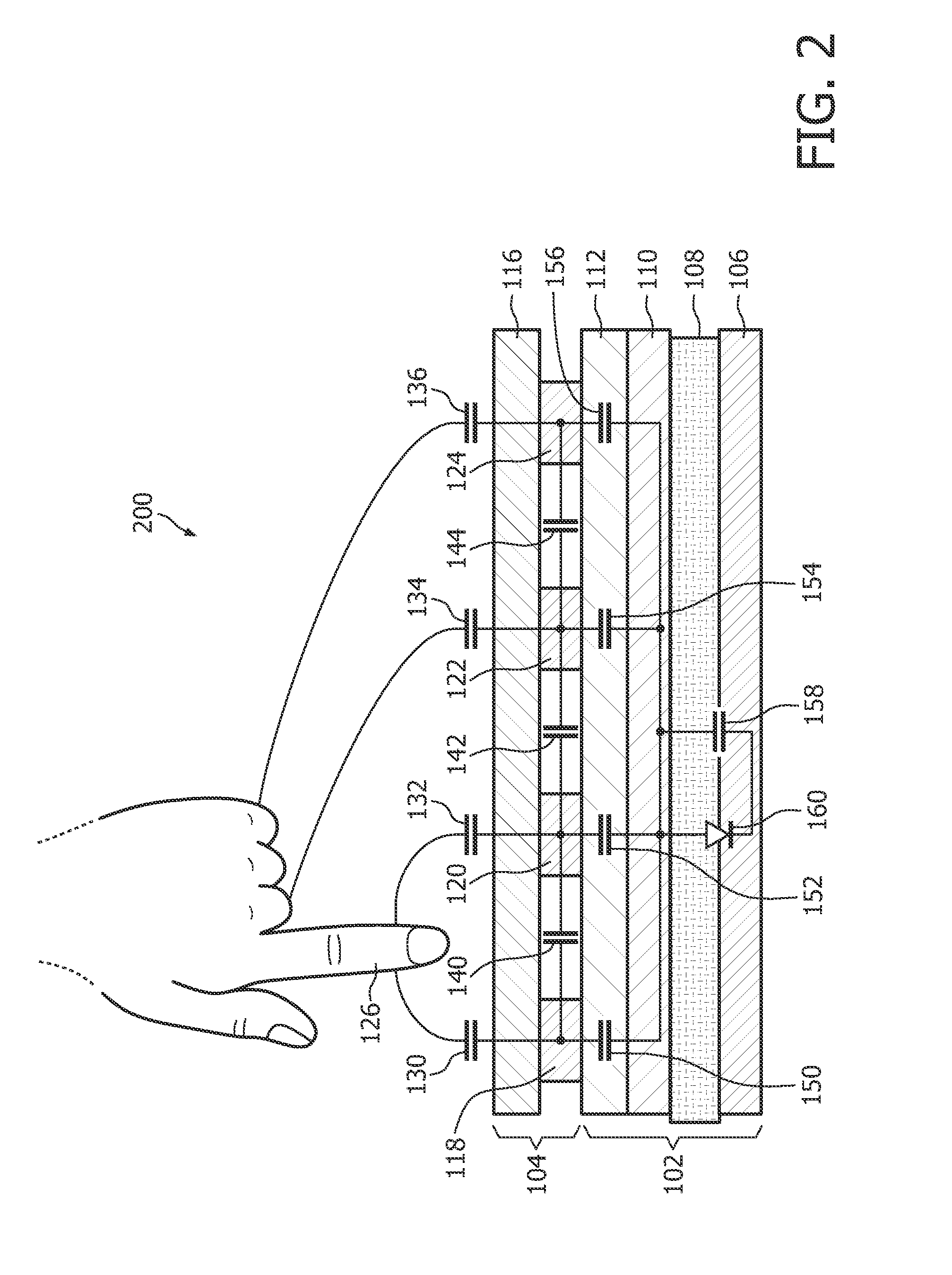
[0035]FIG. 1 shows an OLED device 100 comprised of an OLED means 102 with a laminated NFI sensor foil 104. There is a substrate 112 which is part of the OLED means 102. The substrate 112 has two sides. The OLED means 102 is located on the first side and the NFI sensor 104 is located on the other side. The anode 110 is located directly against the substrate 112. Located next to the anode is the organic layer 108 and on the organic layer 108 is mounted the cathode 106. When a sufficient voltage bias is applied to the anode 110 and cathode 106, light is generated in the organic layer 108. Light then travels through the anode 110 and the substrate 112. On the second side of the substrate, is the NFI sensor foil 104. Located directly immediate to the substrate...


PUM


Abstract

An OLED device comprised of: an OLED means for generating light, two or more conductive elements adapted for conducting current, a first substrate for mounting the OLED means and the two or more conductive elements, wherein the substrate has a first surface and a second surface, wherein the OLED means is in contact with the first surface and the two or more conductive elements are mounted to the second surface.

Description

FIELD OF THE INVENTION[0001]This invention relates to organic light emitting diodes, and in particular to the integration of organic light emitting diodes and near field imaging touch sensors.BACKGROUND OF THE INVENTION[0002]Organic Light Emitting diodes (OLED) devices are comprised of two electrodes and an organic light emitting layer. The organic layer is disposed between the two electrodes. One electrode is the anode and the other electrode is the cathode. The organic layer is structured such that when the anode has a voltage bias that is sufficiently positive relative to the cathode, holes are injected from the anode and electrons are injected from the cathode. The necessary voltage bias depends upon the materials used for the organic layers. The holes and electrons recombine within the organic layer to induce an exited state in a molecule comprising the organic layer. Light is emitted during the process of excited molecules relaxing to their ground state. The anode is typically...

Claims


Application Information

Patent Timeline
Patent Type & Authority Applications(United States)
IPC IPC(8): G06F3/041
CPCG06F3/0412H01L27/323G09G3/32G06F3/044G06F3/0443H10K59/40
Inventor HENTE, DIRK
Owner OLEDWORKS GMBH
Why Eureka
Try Eureka