
Test apparatus and test method

a test apparatus and test method technology, applied in the direction of individual semiconductor device testing, frequency to phase shift conversion, instruments, etc., can solve the problems of test apparatus not being able to supply the device under test with a test signal, the operation clock signal cannot be synchronized between the test apparatus and the device under test, and the inability of the test apparatus to acquire the output signal of the device under tes

Inactive Publication Date: 2011-08-18
ADVANTEST CORP
View PDF7 Cites 17 Cited by
  • Summary
  • Abstract
  • Description
  • Claims
  • Application Information

AI Technical Summary

Benefits of technology

[0016]According to a second aspect related to the innovations herein, provided is a test method for testing a device under test including a plurality of clock domains. The test method comprising generating a rate signal for determining a test period corresponding to an operation period of the device under test; generating a test pattern; for each clock domain, receiving an operation clock signal of the clock domain acquired from a terminal of the device under test included in the clock domain, and detecting a phase difference of the operation clock signal of each domain clock with respect to the rate clock; and for each clock domain, forming a test signal based on the test pattern, according to the phase difference of the corresponding clock domain, to substantially synchronize the test signal with the operation clock signal of the corresponding clock domain.

Problems solved by technology

In this case, the operation clock signals cannot be synchronized between the test apparatus and the device under test.
Therefore, the test apparatus cannot supply the device under test with a test signal and cannot acquire the output signal from the device under test.
However, Patent Document 1 merely describes a waveform shaping method, and does not describe how signals can be synchronized by applying this waveform shaping.
Furthermore, if the device under test has a plurality of clock domains, the phase of the test signal for each clock domain cannot be synchronized.

Method used


Image

  • Test apparatus and test method
  • Test apparatus and test method
  • Test apparatus and test method

Examples


Embodiment Construction

[0026]Hereinafter, an embodiment of the present invention will be described. The embodiment does not limit the invention according to the claims, and all the combinations of the features described in the embodiments are not necessarily essential to means provided by aspects of the invention.

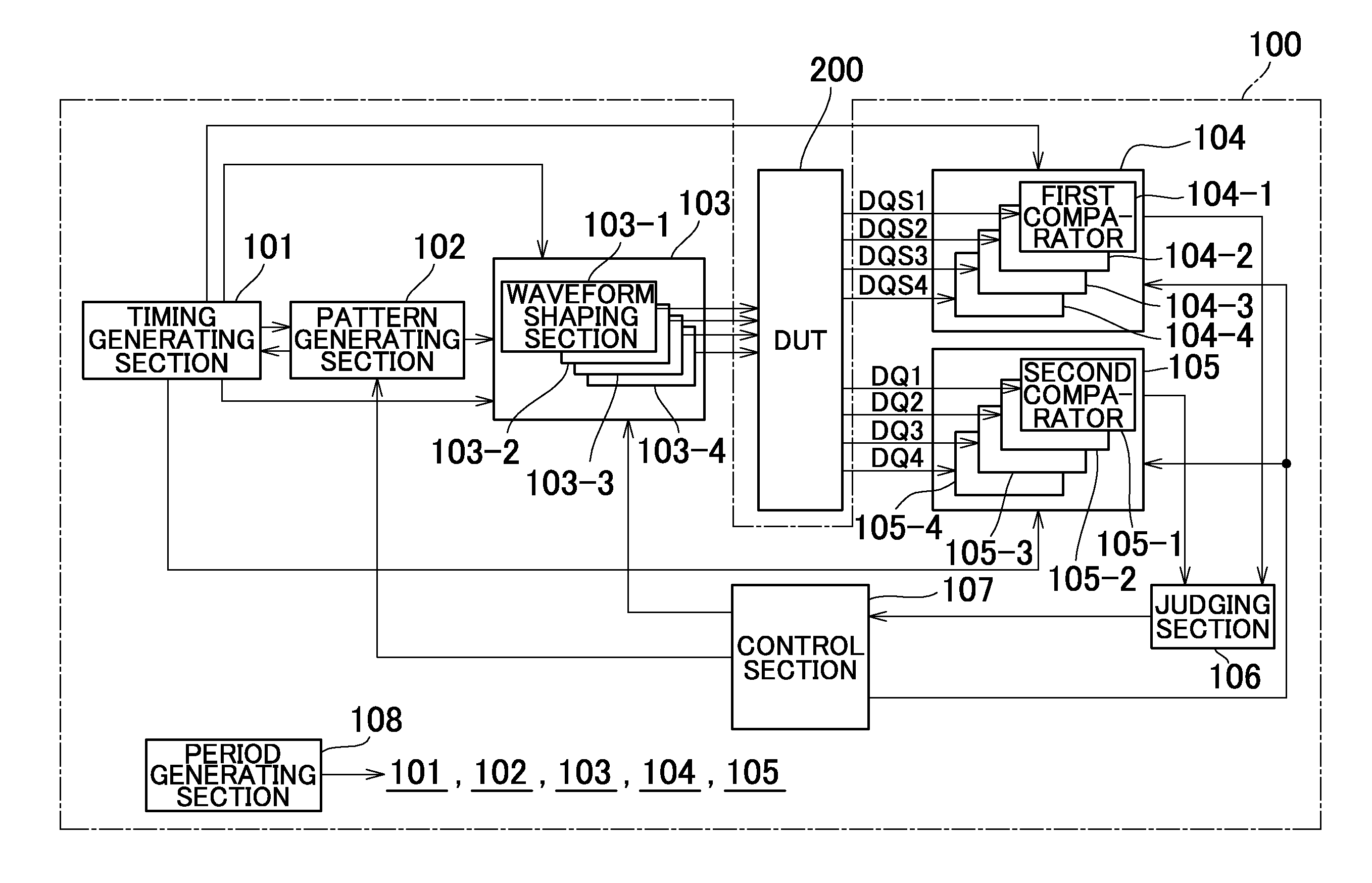
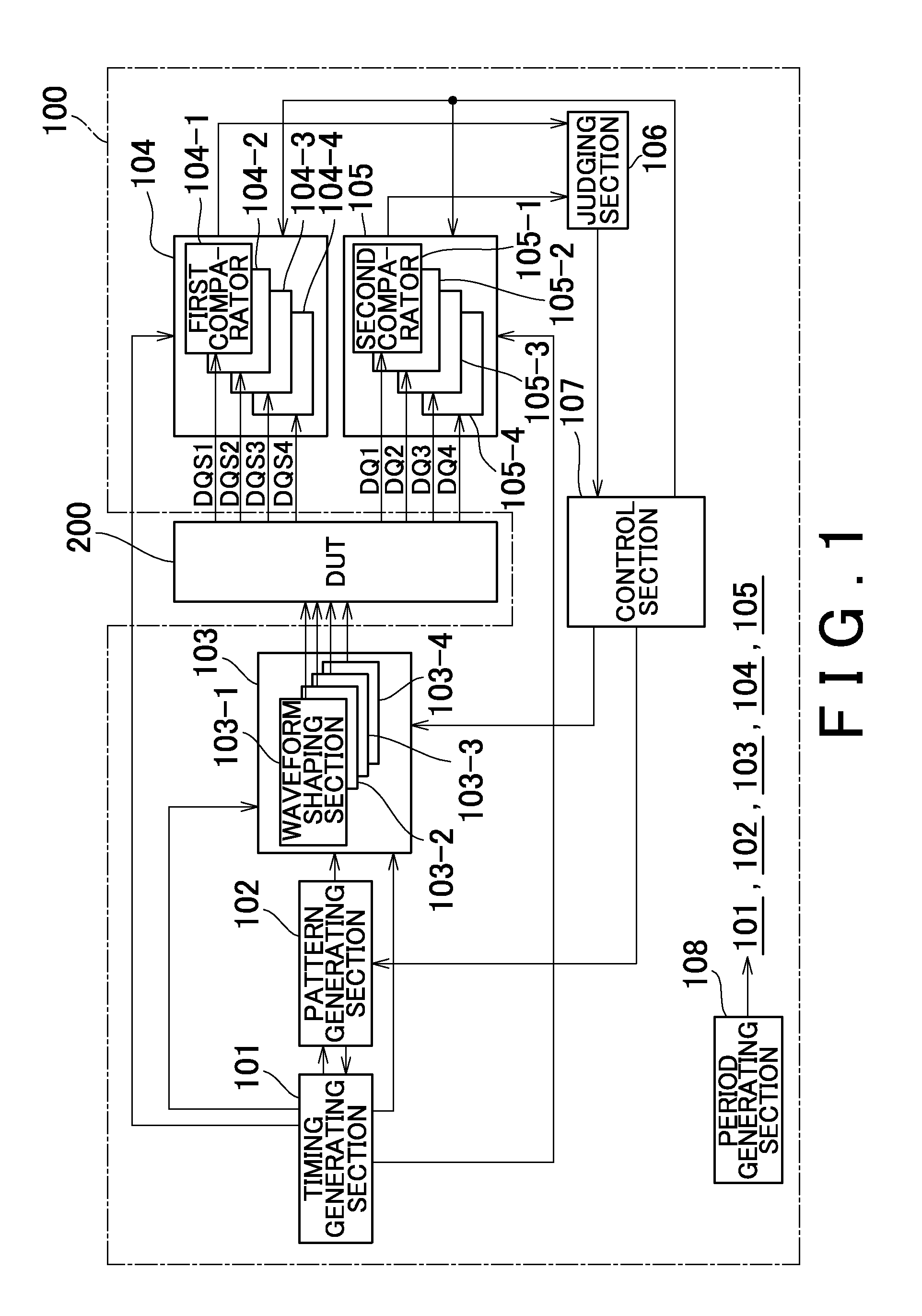
[0027]FIG. 1 shows an overall configuration of the test apparatus 100. The test apparatus 100 detects a phase difference between an operation clock signal of each clock domain of a device under test (DUT) 200 and a rate signal generated by the test apparatus 100. The test apparatus 100 correctly tests the device under test by delaying the test signal input to each clock domain of the DUT 200 according to the corresponding detected phase difference. As a result, the test apparatus 100 can correctly test a device under test that is an electronic device having a plurality of independent oscillation circuits.

[0028]The test apparatus 100 includes a timing generator 101, a pattern generator 102, wavefo...


PUM


Abstract

Provided is a test apparatus and a test method for substantially synchronizing phases of test signals for each of a plurality of clock domains. The test apparatus tests a device under test including a plurality of clock domains. The test apparatus comprises a period generator that generates a rate signal for determining a test period corresponding to an operation period of the device under test; a pattern generator that generates a test pattern; phase comparing sections that, for each clock domain, receive an operation clock signal of the clock domain acquired from a terminal of the device under test included in the clock domain, and detect a phase difference of the operation clock signal of the clock domain with respect to the rate signal; and a plurality of waveform shaping sections that are provided respectively to the clock domains, and that each shape a test signal based on the test pattern, according to the phase difference of the corresponding clock domain, to substantially synchronize the test signal with the operation clock signal of the corresponding clock domain.

Description

BACKGROUND[0001]1. Technical Field[0002]The present invention relates to a test apparatus and a test method. In particular, the present invention relates to a test apparatus and a test method for adjusting timing of test signals supplied to a device under test.[0003]2. Related Art[0004]A test apparatus inputs an operation clock signal to a device under test to cause the device under test to operate according to the operation clock signal. Specifically, the operation clock signals are synchronized between the test apparatus and the device under test, and so the test apparatus can supply the test signal to the device under test based on the operation clock signal or acquire an output signal from the device under test based on the operation clock signal.[0005]Patent Document 1: Japanese Patent Application Publication No. H06-188635[0006]Depending on the type of device under test, operation clock signals can be generated by independent oscillation circuits to operate independently from ...

Claims


Application Information

Patent Timeline
IPC IPC(8): H03L7/00
CPCG01R31/31922G01R31/3183G01R31/319
Inventor YAMADA, TATSUYA
Owner ADVANTEST CORP
Learn More