Touch screen panel and fabricating method thereof

a technology of touch screen panel and fabrication method, which is applied in the manufacture of electric discharge tubes/lamps, instruments, computing, etc., can solve the problems of reducing the fabrication efficiency of touch screen panel and complicated fabrication process, so as to reduce the number of masking processes and ensure stability. , the effect of simplifying the process

Active Publication Date: 2011-08-25
SAMSUNG DISPLAY CO LTD
View PDF7 Cites 31 Cited by
  • Summary
  • Abstract
  • Description
  • Claims
  • Application Information

AI Technical Summary

Benefits of technology

[0011]Aspects of the present invention provide a touch screen panel and a fabricating method thereof, which can simplify processes by reducing the number of mask processes and ensure stability.

Problems solved by technology

Therefore, the fabrication process of the touch screen panel is complicated, and accordingly, the fabrication efficiency of the touch screen panel is lowered.

Method used


Image

  • Touch screen panel and fabricating method thereof
  • Touch screen panel and fabricating method thereof
  • Touch screen panel and fabricating method thereof

Examples


Embodiment Construction

[0027]Reference will now be made in detail to the present embodiments of the present invention, examples of which are illustrated in the accompanying drawings, wherein like reference numerals refer to the like elements throughout. The embodiments are described below in order to explain the present invention by referring to the figures.

[0028]It is to be understood that where is stated herein that a first element is said to be disposed or formed “on” or “in” or “connected to” a second element, the first element can directly contact the second element, or can be separated from the second element by one or more other elements located therebetween. In contrast, when an element is referred to as being disposed or formed “directly on” or “directly connected to” another element, there are no intervening elements present.

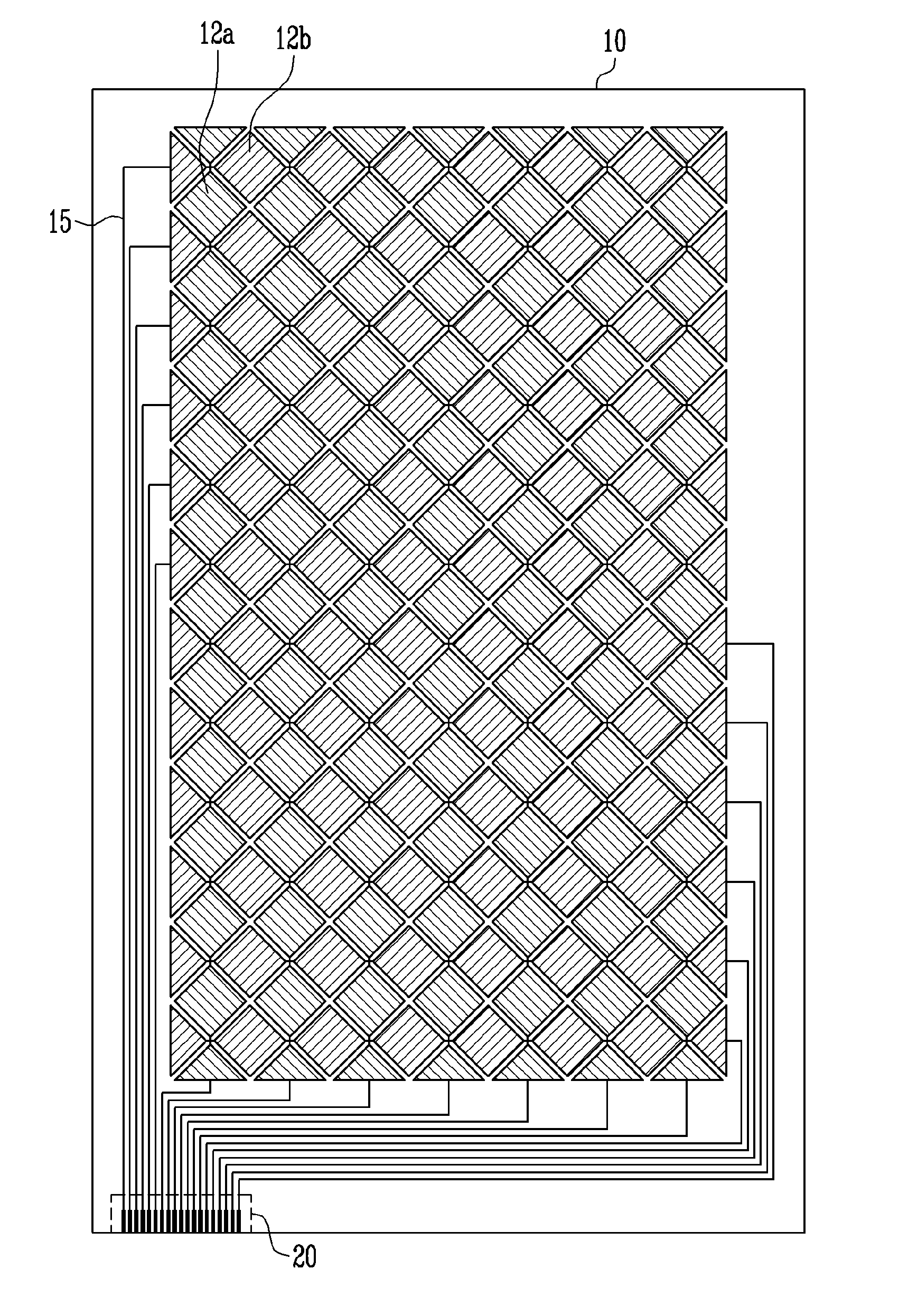
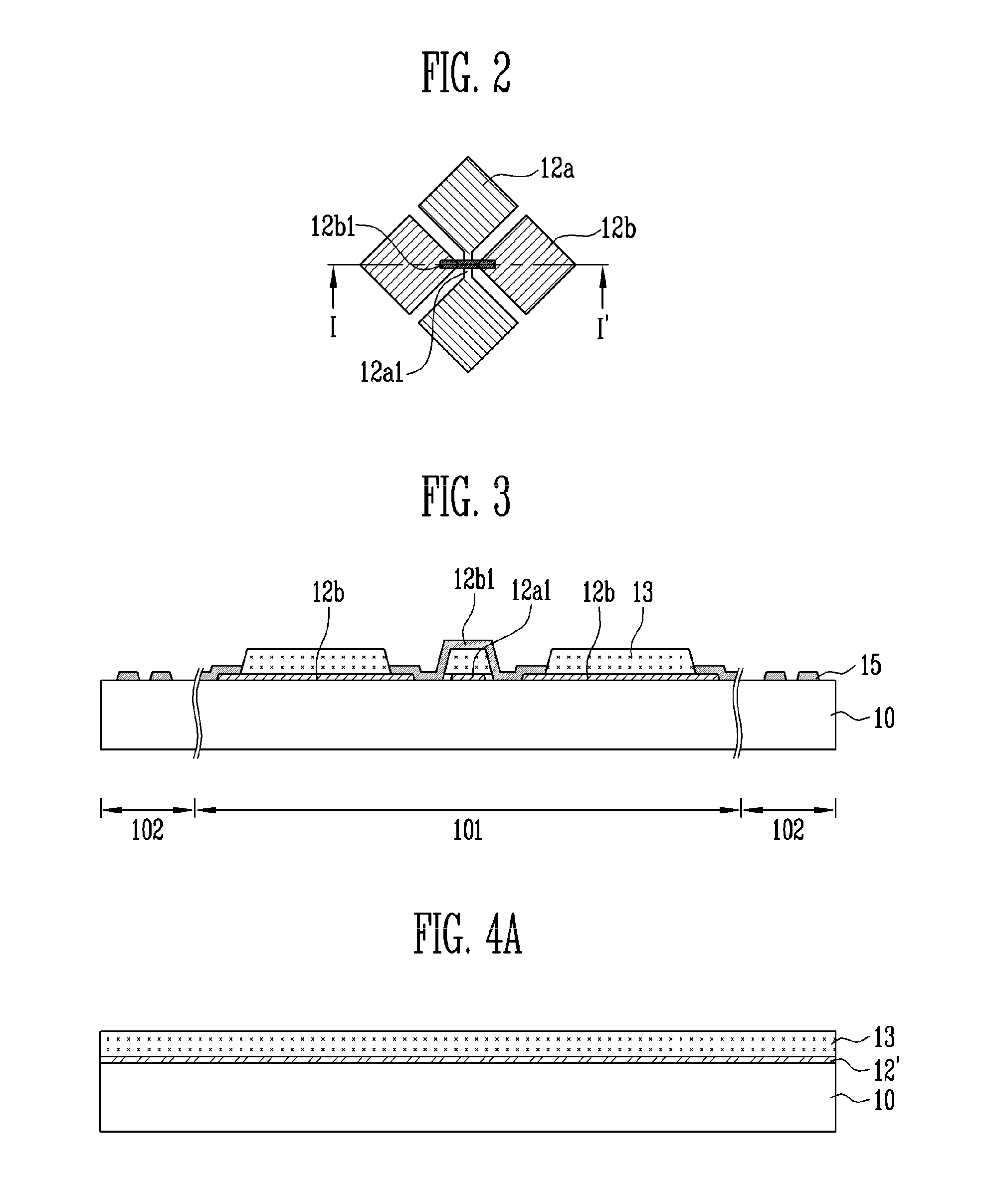
[0029]FIG. 1 is a plan view schematically showing a touch screen panel according to an embodiment of the present invention. FIG. 2 is a main part plan view showing sensing p...


PUM


Abstract

A fabricating method of a touch screen panel, a transparent electrode layer and an insulating layer which are sequentially formed on a same surface of a transparent substrate. The transparent electrode layer and the insulating layer are co-patterned using a halftone mask to form a plurality of first sensing patterns connected along a first direction, a plurality of second sensing patterns having separated patterns between the first sensing patterns, and the insulating layer positioned on the first and second sensing patterns to expose regions of the second sensing patterns. A conductive layer is formed on the transparent substrate on which the first and second sensing patterns and the insulating layer are formed. The conductive layer is patterned to form second connection patterns allowing the second sensing patterns to be connected along a second direction through the exposed regions of the second sensing patterns.

Description

CROSS-REFERENCE TO RELATED APPLICATION[0001]This application claims the benefit of Korean Patent Application No. 10-2010-0015702, filed Feb. 22, 2010, in the Korean Intellectual Property Office, the disclosure of which is incorporated herein by reference.BACKGROUND[0002]1. Field[0003]Aspects of the present invention relate to a touch screen panel provided to an image display device and the like, and a fabricating method thereof.[0004]2. Description of the Related Art[0005]A touch screen panel is an input device that allows a user's instruction to be inputted by selecting an instruction content displayed on a screen such as an image display device with a user's hand or object.[0006]To this end, the touch screen panel is formed on a front face of the image display device to convert a contact position into an electrical signal. Here, the user's hand or object is directly in contact with the touch screen panel at the contact position. Accordingly, the instruction content selected at the...

Claims


Application Information

Patent Timeline
Patent Type & Authority Applications(United States)
IPC IPC(8): G06F3/041H01J9/00
CPCG06F3/044G06F3/0412G06F3/0446G06F2203/04103G06F2203/04111
Inventor JUN, WOO-SIK
Owner SAMSUNG DISPLAY CO LTD
Why Eureka
Try Eureka