Supercharge Your Innovation With Domain-Expert AI Agents!

Redundancy data storage circuit, redundancy data control method and repair determination circuit of semiconductor memory

a data storage circuit and data control technology, applied in the field of semiconductor memory, can solve the problem that no new repair address can be stored after packaging

Inactive Publication Date: 2011-08-25
SK HYNIX INC
View PDF10 Cites 2 Cited by
  • Summary
  • Abstract
  • Description
  • Claims
  • Application Information

AI Technical Summary

Benefits of technology

The present invention is related to a semiconductor memory that can change a repair address and store a new repair address even after packaging. Additionally, the invention provides a method for writing redundancy data in a semiconductor memory without the need for a cutting process. The invention also includes a redundancy data control method that allows for the efficient storage and output of redundancy data in response to a test signal. Finally, the invention includes a repair determination circuit that can detect and output redundancy addresses for comparison with column addresses, and ultimately determine if a repair is needed. Overall, the invention improves the efficiency and accuracy of semiconductor memory repair processes.

Problems solved by technology

Consequently, the conventional technique presents problems, inter alia, in that no new repair address can be stored after packaging since the metal fuse has been physically cut.

Method used


Image

  • Redundancy data storage circuit, redundancy data control method and repair determination circuit of semiconductor memory
  • Redundancy data storage circuit, redundancy data control method and repair determination circuit of semiconductor memory
  • Redundancy data storage circuit, redundancy data control method and repair determination circuit of semiconductor memory

Examples


Embodiment Construction

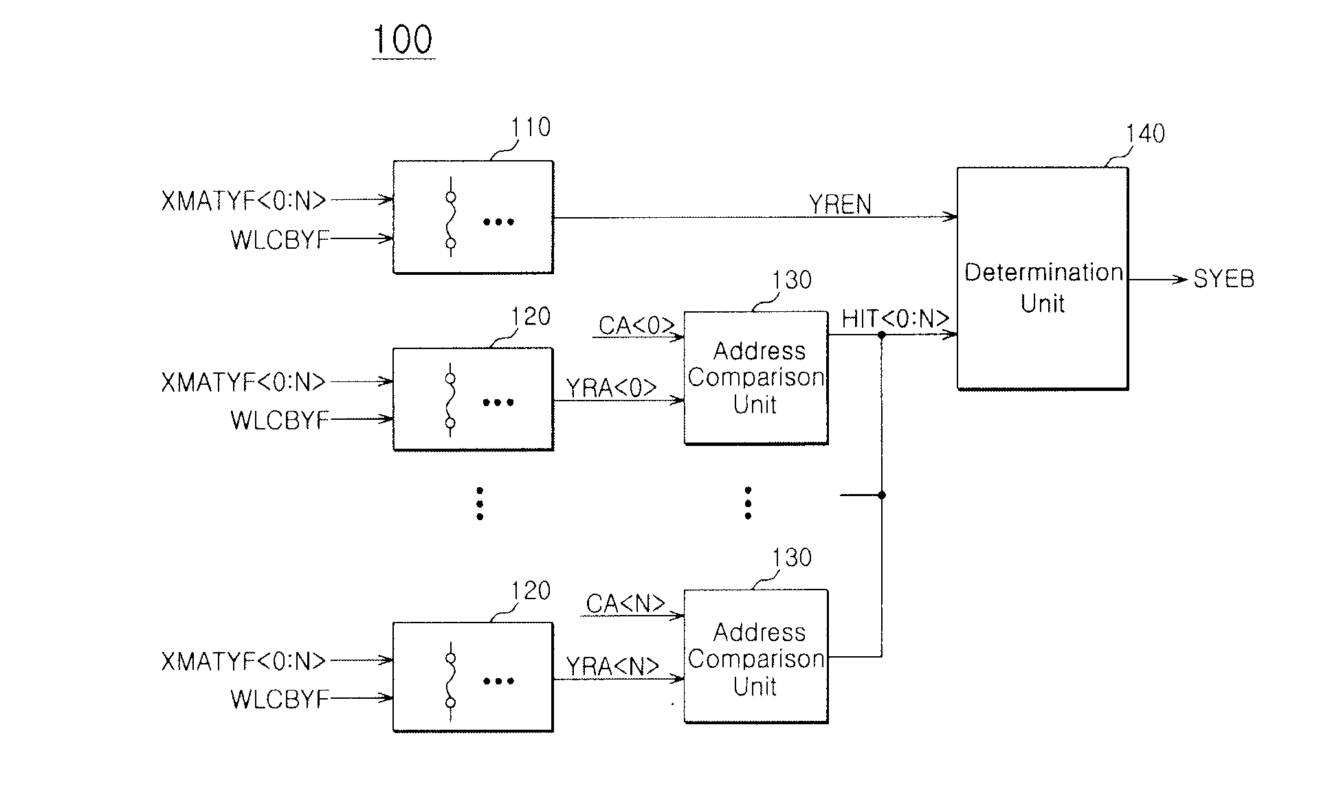
[0023]Hereinafter, a redundancy data storage circuit, a redundancy data control method, and a repair determination circuit of a semiconductor memory according to embodiments of the present invention will be described below with reference to the accompanying drawings.

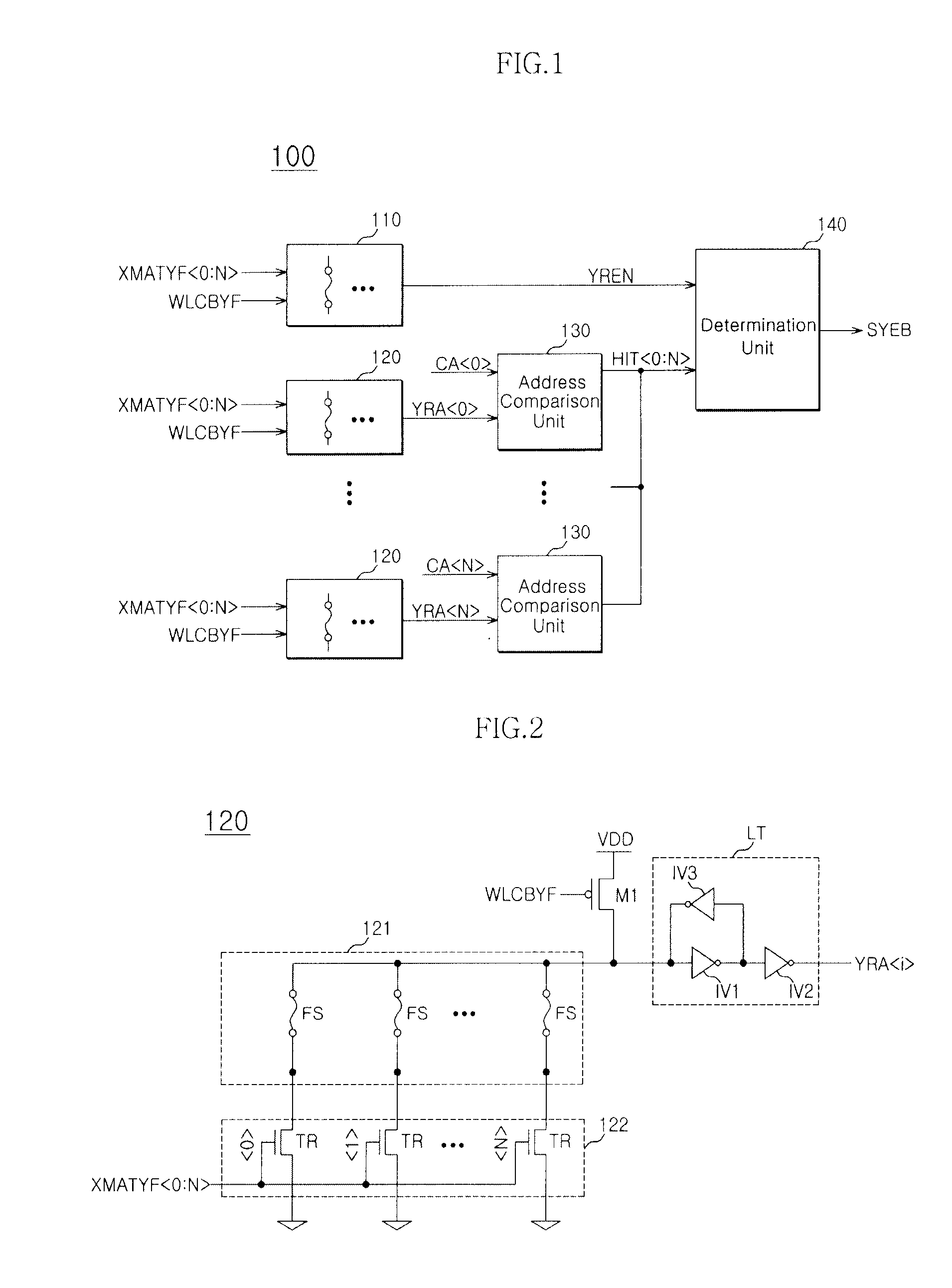
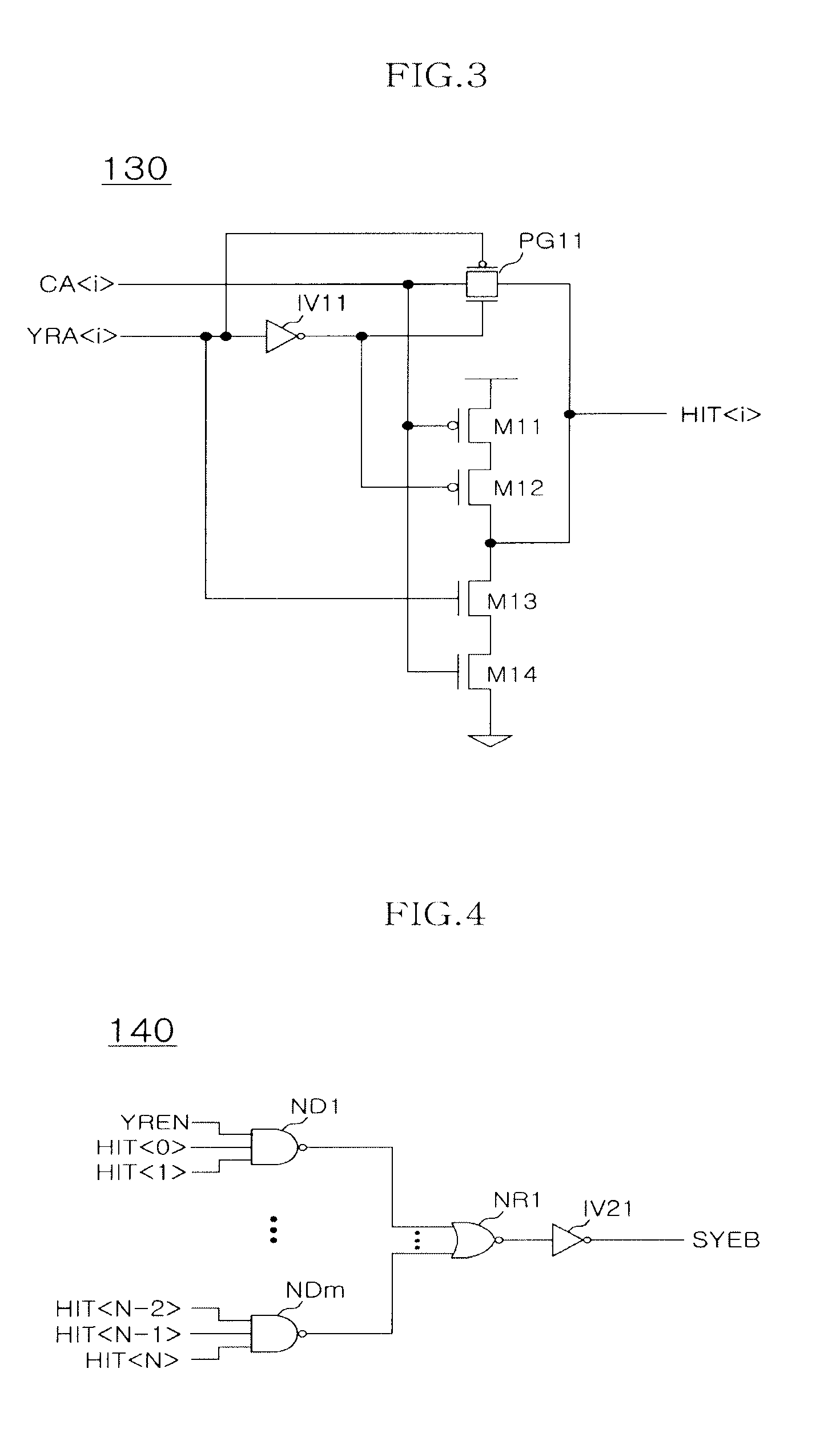
[0024]Referring to FIG. 1, a repair determination circuit 100 of a semiconductor memory includes an enable fuse set 110, a plurality of address fuse sets 120, a plurality of address comparison units 130, and a determination unit 140.

[0025]The enable fuse set 110 is configured to receive active signals XMATYF and WLCBYF and output a fuse set enable signal YREN for informing whether or not to use a fuse setting circuit.

[0026]The active signals XMATYF are signals which include information regarding activation of a unit cell array, that is, a cell mat divided in a row direction. The active signal WLCBYF is a signal which has information regarding activation of a word line. The active signal WLCBYF has a high level when the w...


PUM


Abstract

A redundancy data storage circuit of a semiconductor memory includes a memory cell array; a write driver configured to write redundancy data in the memory cell array in response to a test signal; and a sense amplifier configured to detect and output the redundancy data written in the memory cell array in response to a read signal.

Description

CROSS-REFERENCES TO RELATED APPLICATION[0001]The present application claims priority under 35 U.S.C. §119(a) to Korean application number 10-2010-0016743, filed on Feb. 24, 2010, in the Korean Intellectual Property Office, which is incorporated herein by reference in its entirety as set forth in full.BACKGROUND[0002]1. Technical Field[0003]The present invention relates generally to a semiconductor memory, and more particularly to a redundancy data storage circuit, a redundancy data control method, and a repair determination circuit of a semiconductor memory.[0004]2. Related Art[0005]The circuit design of a semiconductor memory includes a provision to allow a repair operation, which will replace failed memory cells with redundancy cells.[0006]That is, the semiconductor memory is designed with a repair determination circuit that stores the address data needing repair (hereinafter, “the repair address”), determines whether any address externally inputted corresponds to the stored repai...

Claims


Application Information

Patent Timeline
Patent Type & Authority Applications(United States)
IPC IPC(8): G11C29/04
CPCG11C11/16G11C29/812G11C29/785
Inventor SEO, WOO HYUNRHO, KWANG MYOUNG
Owner SK HYNIX INC
Features
  • R&D
  • Intellectual Property
  • Life Sciences
  • Materials
  • Tech Scout
  • Unparalleled Data Quality
  • Higher Quality Content
  • 60% Fewer Hallucinations
Learn More