Integrated method for forming high-k metal gate finfet devices

Active Publication Date: 2011-08-25
TAIWAN SEMICON MFG CO LTD
View PDF23 Cites 9 Cited by
  • Summary
  • Abstract
  • Description
  • Claims
  • Application Information

AI Technical Summary

Benefits of technology

[0012]In one embodiment, the metal gate structure comprises a high-k gate dielectric, a metal gate film over the high-k gate dielectric and a polysilicon gate over the metal gate film, but other structures may be used in other exemplary embodiments. Prior to forming any spacers alongside the metal gate structure, the method provides for forming a thin nitride layer over the semiconductor fin and over the metal gate structure and implanting dopant impurities into the semiconductor fin through the thin nitride layer, the implanting comprising at least

Problems solved by technology

It can be seen that the limitations of conventional processing cause the damage and recession of the semiconductor

Method used


Image

  • Integrated method for forming high-k metal gate finfet devices
  • Integrated method for forming high-k metal gate finfet devices
  • Integrated method for forming high-k metal gate finfet devices

Examples


Example

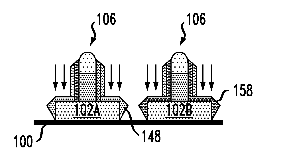
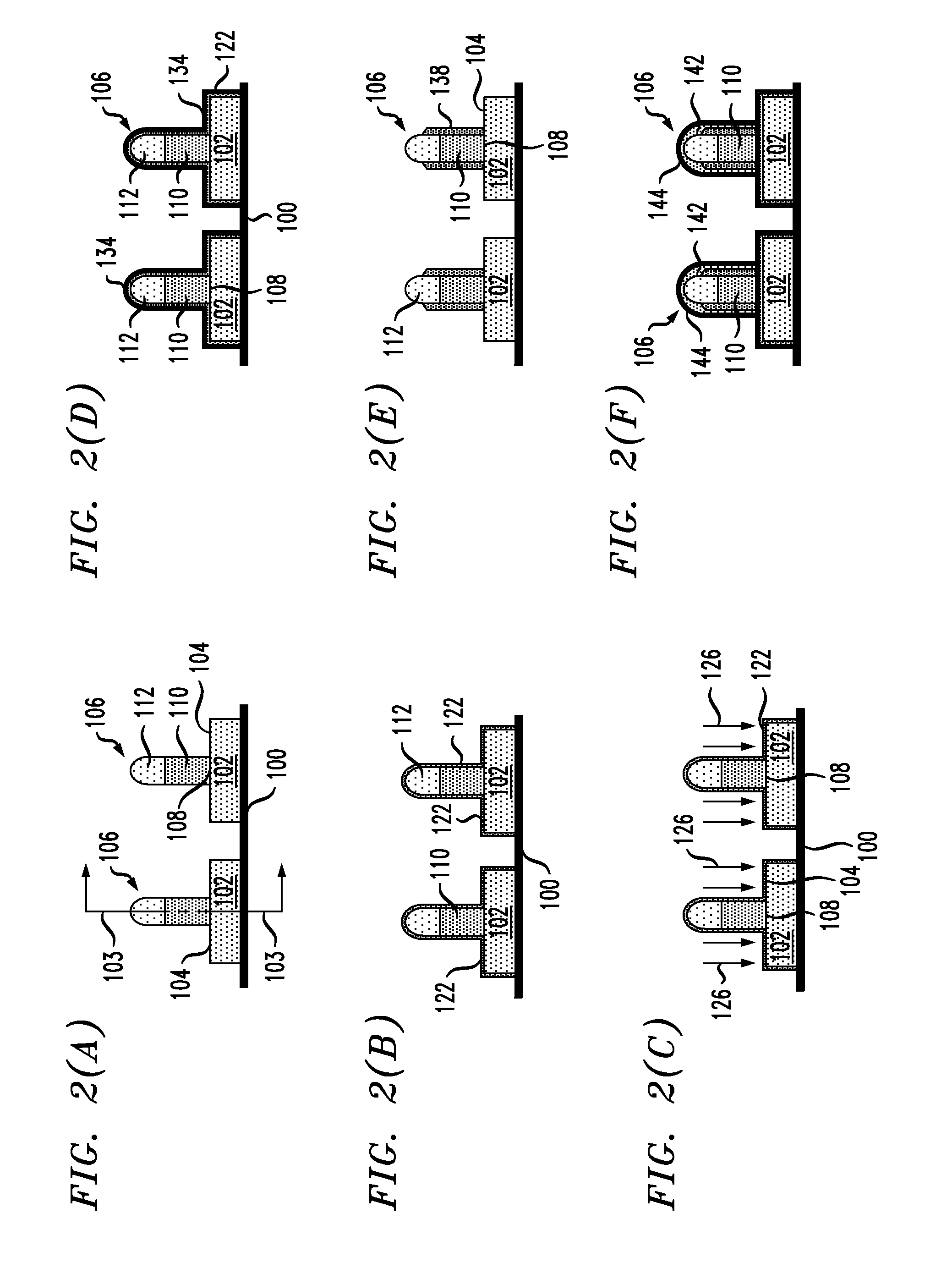
[0018]The present invention provides for forming a high-k or other metal gate structure over a semiconductor fin and then forming a nitride layer covering the gate and the semiconductor fin, using two separate deposition operations, the first forming a very thin nitride film. Implantation operations such as a lightly doped drain, LDD implant operation and a packet, PKT, implant operation are carried out in between the two nitride film deposition operations. The thin nitride film may be SiNx or SiCNx and precludes the need to form wide spacers alongside the gate structure prior to implant, which are needed in conventional processing to avoid damaging the high-k gate dielectric and metal formed on the fin. The second nitride film is a SiCNx film formed by PECVD, LPCVD or ALD and includes low wet etch rates in H3PO4 and dilute HF acid which enables further processing operations to be carried out without damaging the nitride films or underlying structures and without requiring the forma...


PUM


Abstract

Provided is a high-k metal gate structure formed over a semiconductor fin. A nitride layer is formed over the gate structure and the semiconductor fin, using two separate deposition operations, the first forming a very thin nitride film. Implantation operations such as an LDD or a PKT implant, are carried out in between the two nitride film deposition operations. The first nitride film may be SiNx or SiCNx and the second nitride film is SiCNx with a low wet etch rate in H3PO4 and dilute HF acid. The nitride films may be combined to form low wet etch rate spacers enabling further processing operations to be carried out without damaging underlying structures and without requiring the formation of further dummy spacers. Further processing operations include epitaxial silicon/SiGe processing sequences and source/drain implanting operations carried out with the low etch rate spacers intact.

Description

FIELD OF THE INVENTION[0001]The present invention relates, most generally, to semiconductor device fabrication and, more particularly, to a method for fabricating high-k metal gate transistors over semiconductor fin structures, and the devices so formed.BACKGROUND[0002]Semiconductor fins are widely used in advanced semiconductor manufacturing technology because of the increased integration levels they provide. For example, when transistor devices such as FinFET, fin Field Effect Transistor, devices are formed they provide a gate width that may be larger, by an order of magnitude, than the gate width of the transistor formed on the same substrate section in which the semiconductor fin is formed because the gate extends over the top and sides of the fins, all of which serve as channels. Semiconductor fins have high aspect ratios and require advanced and dedicated processing operations to forming working FinFET or other devices using the semiconductor fins.[0003]When these devices are ...

Claims


Application Information

Patent Timeline
IPC IPC(8): H01L21/336
CPCH01L29/66803H01L29/66795
Inventor LIN, CHIA-PINHUANG, WEN-SHEHGAN, TIAN-CHOYHUNG, CHIA-LUNGLIN, HSIEN-CHINLIN, SHYUE-SHYH
Owner TAIWAN SEMICON MFG CO LTD
Why Eureka
Try Eureka