Processing method for wafer having embedded electrodes

Inactive Publication Date: 2012-10-04
DISCO CORP
View PDF3 Cites 12 Cited by
  • Summary
  • Abstract
  • Description
  • Claims
  • Application Information

AI Technical Summary

Benefits of technology

[0013]Accordingly, the etching rate to the silicon dioxide (SiO2) film covering the electrode in the second etching step

Problems solved by technology

Accordingly, there is a problem such that the silicon dioxide (SiO2) film as an insulating film covering the copper (Cu) electrodes is etched by potassium hydroxide (KOH) to cause a reduction in insulation quality between the silicon (Si) substrate and the copper (Cu) electrodes.
On the

Method used


Image

  • Processing method for wafer having embedded electrodes
  • Processing method for wafer having embedded electrodes
  • Processing method for wafer having embedded electrodes

Examples


Example

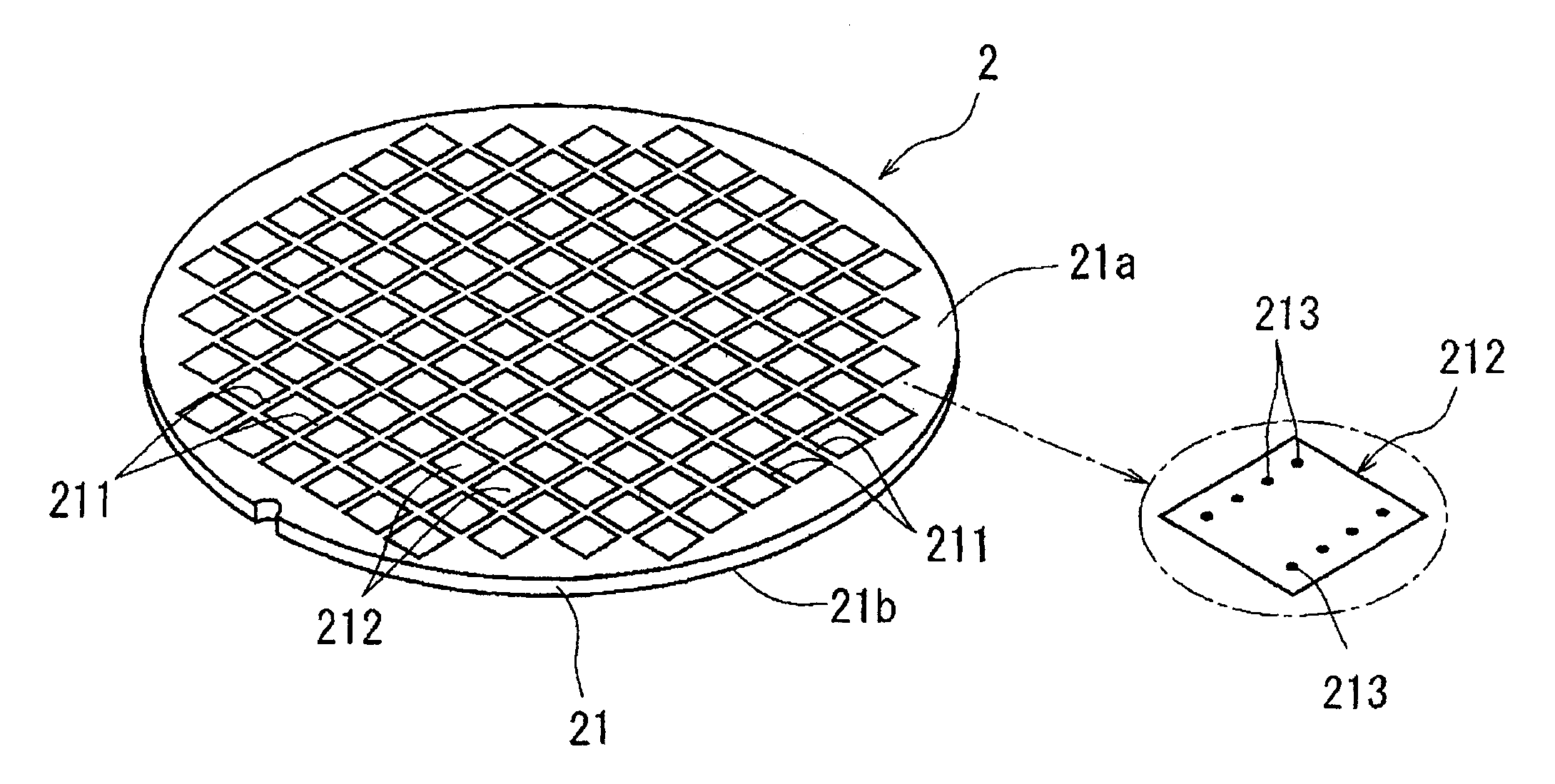
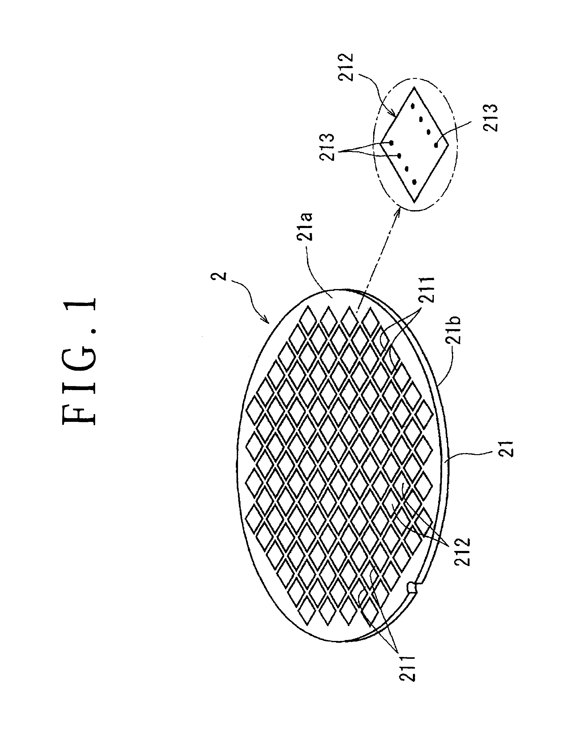
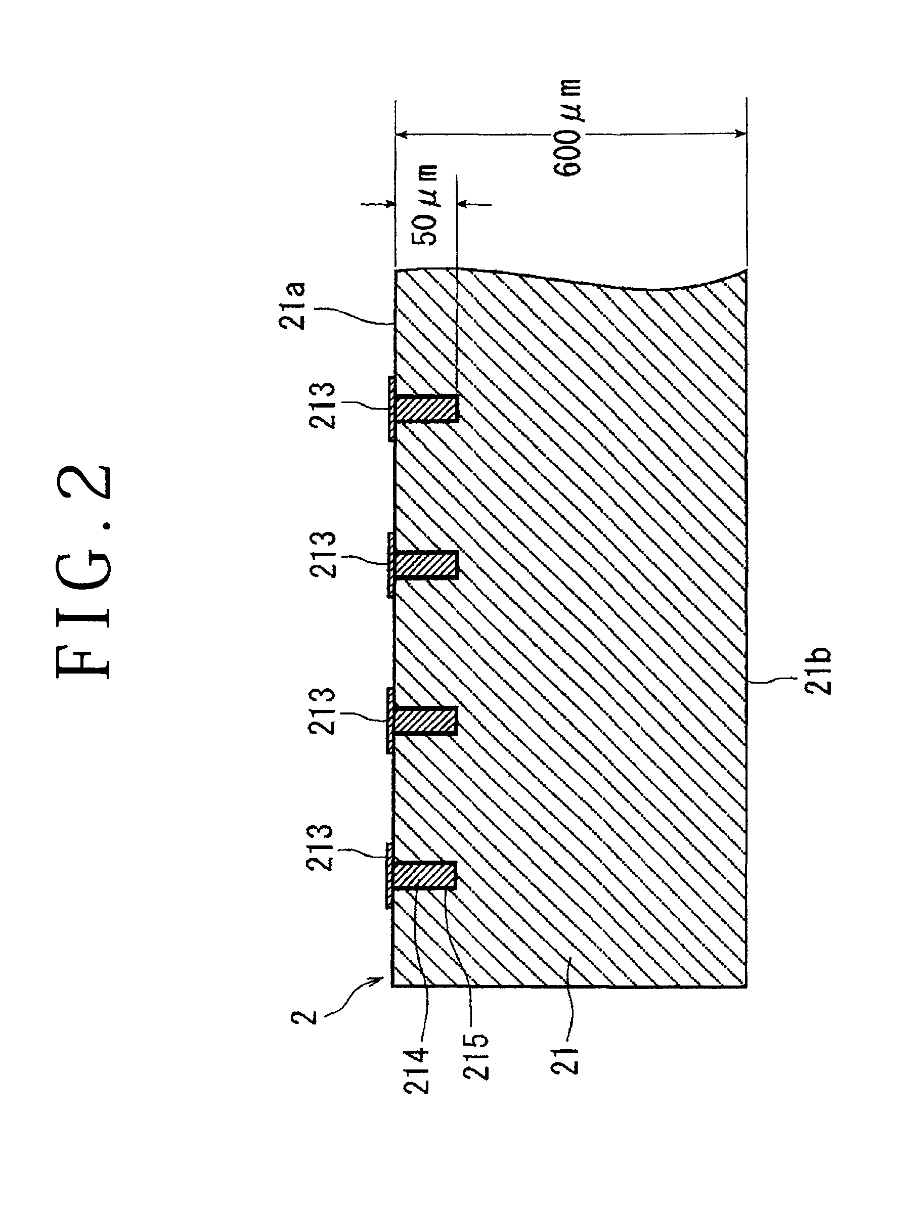
[0026]A preferred embodiment of the wafer processing method according to the present invention will now be described in detail with reference to the attached drawings. FIG. 1 is a perspective view of a wafer 2 to be processed by the wafer processing method according to the present invention. The wafer 2 shown in FIG. 1 is formed from a silicon (Si) substrate 21 having a thickness of 600 μm, for example. The silicon (Si) substrate 21 has a front side 21a and a back side 21b. A plurality of crossing streets 211 are formed on the front side 21a of the silicon (Si) substrate 21 to thereby partition a plurality of rectangular regions where a plurality of devices 212 such as ICs and LSIs are respectively formed. A plurality of bonding pads 213 are provided on the front side of each device 212. As shown in FIG. 2, a plurality of copper (Cu) electrodes 214 respectively connected to the bonding pads 213 are embedded in the silicon (Si) substrate 21 of the wafer 2. Each copper (Cu) electrode ...


PUM


Abstract

A wafer processing method which includes a protective member attaching step of attaching a protective member to the front side of the wafer, a back grinding step of grinding the back side of the silicon (Si) substrate of the wafer so as not to expose electrodes to the back side of the silicon (Si) substrate, and an etching step of etching the back side of the silicon (Si) substrate by using an etching liquid to thereby expose the electrodes to the back side of the silicon (Si) substrate. The etching liquid includes a first etching liquid having a high etching rate to silicon (Si) and a second etching liquid capable of etching silicon (Si) and having a low etching rate to silicon dioxide (SiO2).

Description

BACKGROUND OF THE INVENTION[0001]1. Field of the Invention[0002]The present invention relates to a wafer processing method for processing a wafer including a silicon substrate and a plurality of devices formed on the front side of the silicon substrate, wherein each device is provided with a bonding pad, and an electrode is embedded in the silicon substrate so as to be connected to the bonding pad.[0003]2. Description of the Related Art[0004]In a semiconductor device fabrication process, a plurality of crossing division lines called streets are formed on the front side of a substantially disk-shaped silicon (Si) substrate to partition a plurality of regions where a plurality of semiconductor devices such as ICs and LSIs are respectively formed, thus obtaining a wafer including the silicon (Si) substrate and the plural semiconductor devices formed on the front side of the silicon (Si) substrate. The wafer is cut along the streets to thereby divide the regions where the semiconductor ...

Claims


Application Information

Patent Timeline
IPC IPC(8): H01L21/306
CPCH01L21/304H01L21/30604B24B7/228H01L21/30625H01L21/6708H01L21/30608
Inventor NISHIDA, YOSHITERU
Owner DISCO CORP
Why Eureka
Try Eureka