Data output circuit and data output method thereof

a data output circuit and data technology, applied in pulse manipulation, pulse automatic control, pulse technique, etc., can solve the problems of data distortion, data margin may be reduced, output data of semiconductor memory devices may be distorted, etc., to improve jitter characteristics and ensure data margin

Inactive Publication Date: 2011-09-01
SK HYNIX INC
View PDF1 Cites 4 Cited by
  • Summary
  • Abstract
  • Description
  • Claims
  • Application Information

AI Technical Summary

Benefits of technology

[0027]An embodiment of the present invention is directed to a data output circuit capable of improving jitter characteristic and ensuring data margin and a data output method thereof.

Problems solved by technology

If a duty ratio of a clock is not accurately controlled, data margin may not be ensured, causing distortion of data.
Consequently, data margin may be reduced and thus output data of the semiconductor memory device may be distorted.
However, while the first internal clocks RCLK_DLL1 and FCLK_DLL1 pass through several internal circuits including the repeater 130, their duty ratios may be distorted by external noises, distortion of transmission lines, or PVT variations.
Consequently, data margin is reduced and jitter characteristic is degraded, resulting in distortion of the output data DQ.

Method used


Image

  • Data output circuit and data output method thereof
  • Data output circuit and data output method thereof
  • Data output circuit and data output method thereof

Examples


Embodiment Construction

[0043]Exemplary embodiments of the present invention will be described below in more detail with reference to the accompanying drawings. The present invention may, however, be embodied in different forms and should not be construed as limited to the embodiments set forth herein. Rather, these embodiments are provided so that this disclosure will be thorough and complete, and will fully convey the scope of the present invention to those skilled in the art. Throughout the disclosure, like reference numerals refer to like parts throughout the various figures and embodiments of the present invention.

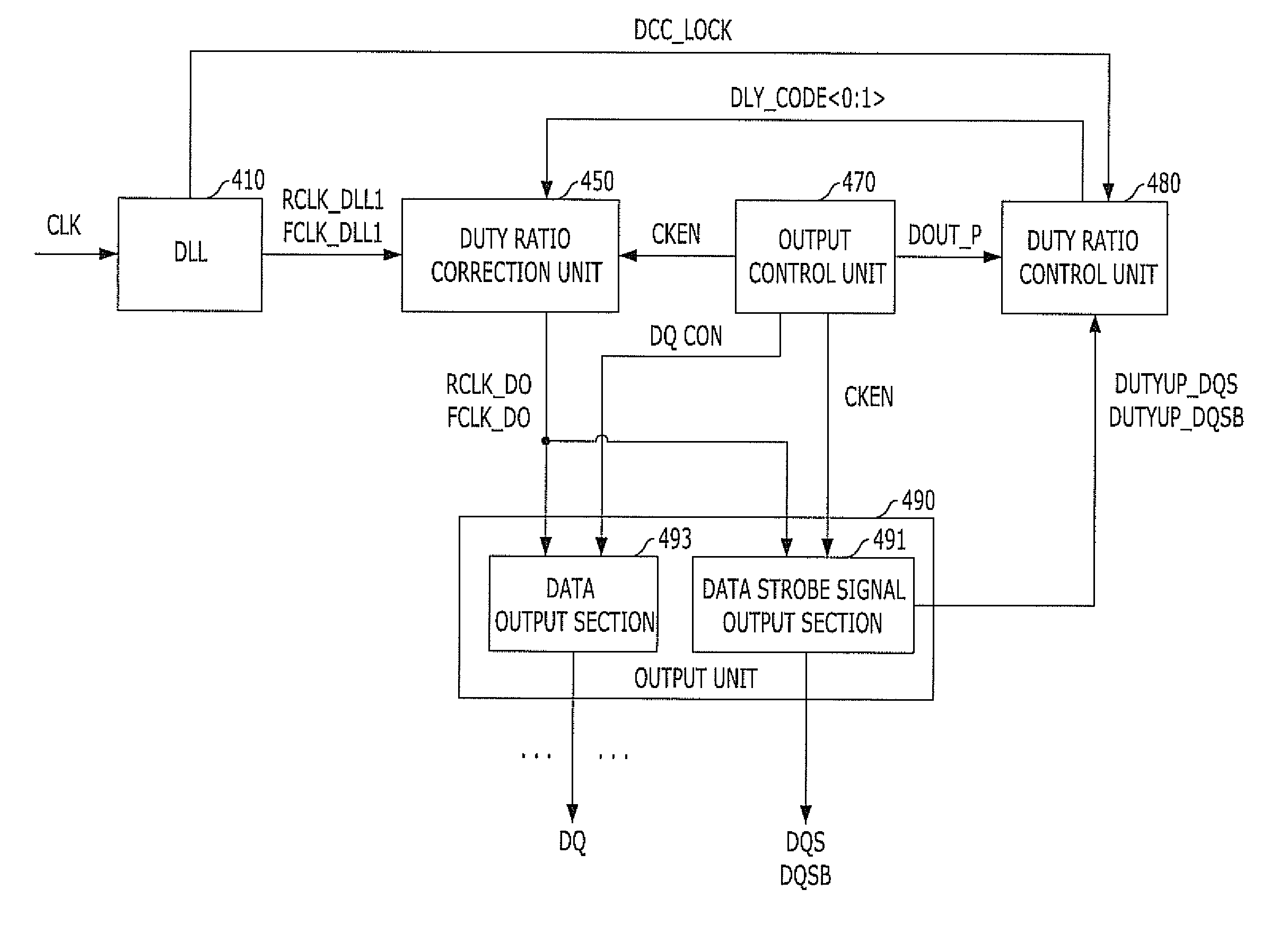
[0044]FIG. 4 is a configuration diagram of a data output circuit in accordance with an embodiment of the present invention.

[0045]Referring to FIG. 4, a data output circuit in accordance with an embodiment of the present invention includes a DLL 410, a duty ratio correction unit 450, an output control unit 470, a duty ratio control unit 480, and an output unit 490.

[0046]The DLL 410 compares a...


PUM


Abstract

A data output circuit and a data output method thereof are provided. The data output circuit includes a delay locked loop, a duty ratio correction block, and an output unit. The delay locked loop corrects a duty ratio of a first internal clock. The delay locked loop includes a correction enable signal output unit configured to output a correction enable signal when the operation of correcting the duty ratio of the first internal clock is completed. The duty ratio correction block corrects the duty ratio of the first internal clock by using a duty ratio detection signal in response to the correction enable signal, and outputs the corrected first internal clock as an output clock. The output unit detects a duty ratio of the output clock, generates the duty ratio detection signal to the duty ratio correction block, and outputs a data strobe signal in response to the output clock.

Description

CROSS-REFERENCE TO RELATED APPLICATIONS[0001]The present application claims priority of Korean Patent Application No. 10-2010-0017980, filed on Feb. 26, 2010, which is incorporated herein by reference in its entirety.BACKGROUND OF THE INVENTION[0002]Exemplary embodiments of the present invention relate to a data output circuit of a semiconductor memory device, and more particularly, to a data output circuit for correcting a duty ratio of an output clock, and a data output method thereof.[0003]Synchronous semiconductor memory devices are designed to operate in synchronization with an external clock. Double data rate (DDR) synchronous memory devices successively process two-bit data in one clock cycle in synchronization with the rising and falling edges of an external clock. The DDR synchronous memory devices may use a delay locked loop (DLL) to implement accurate data input / output timings.[0004]In such synchronous semiconductor memory devices, data are inputted and outputted based on...

Claims


Application Information

Patent Timeline
Patent Type & Authority Applications(United States)
IPC IPC(8): H03L7/06H03K3/017
CPCH03K5/1565H03K5/04H03L7/0816
Inventor CHUNG, JIN-IL
Owner SK HYNIX INC
Why Eureka
Try Eureka