Semiconductor device

A semiconductor and device technology, applied in the field of semiconductor devices, can solve the problem of increasing power consumption of driving circuits, and achieve the effects of suppressing changes in power supply voltage, improving jitter characteristics, and suppressing changes

Inactive Publication Date: 2017-03-01
RENESAS ELECTRONICS CORP
View PDF10 Cites 0 Cited by
  • Summary
  • Abstract
  • Description
  • Claims
  • Application Information

AI Technical Summary

Problems solved by technology

But there is such a problem that since the signal level is set according to the current, the drive circuit that processes the CML signal increases the power consumption

Method used


Image

  • Semiconductor device
  • Semiconductor device
  • Semiconductor device

Examples


no. 1 example

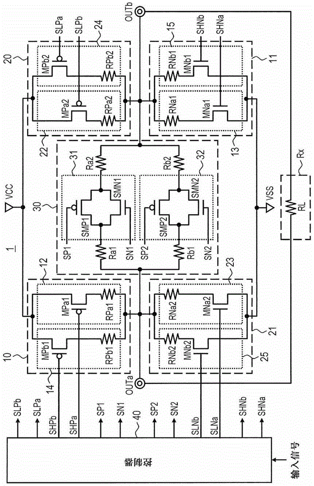
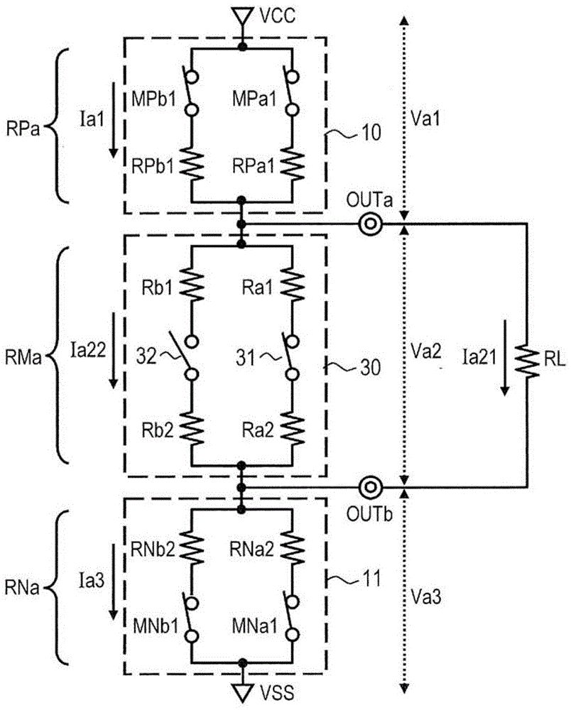
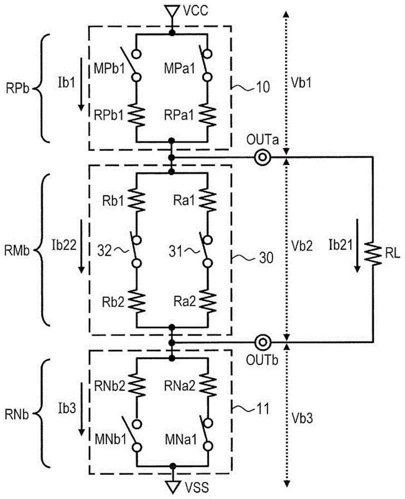
[0026] Embodiments of the present invention will be described below with reference to the drawings. figure 1 A block diagram of the semiconductor device 1 according to the first embodiment is shown. figure 1 A driving circuit and a controller for controlling the driving circuit in which the present invention focuses on the semiconductor device are shown. That is, the semiconductor device 1 includes many circuits that are not shown except the driving circuit. Such as figure 1 As shown in , the semiconductor device 1 includes a first driver 10 , a second driver 11 , a third driver 20 , a fourth driver 21 , a variable resistor 30 and a controller 40 . The semiconductor device 1 also includes a first output terminal OUTa and a second output terminal OUTb. The semiconductor device 1 outputs a differential signal having an amplitude corresponding to the input signal through the first output terminal OUTa and the second output terminal OUTb. The differential signal is transmitted...

no. 2 example

[0103] Figure 6 A block diagram of a semiconductor device 2 according to the second embodiment is shown in . In the semiconductor device 1 according to the first embodiment, each of the plurality of drivers has a resistor for determining output impedance in an on state. However, if Figure 6 As shown in , in the semiconductor device 2 according to the second embodiment, a pair of resistors is shared by two drivers.

[0104] Accordingly, the semiconductor device 2 includes the first driver 50 , the second driver 51 , the third driver 60 and the fourth driver 61 in other configurations such as the first driver 10 , the second driver 11 , the third driver 20 and the fourth driver 21 .

[0105] The first driver 50 includes a first output setting unit 52 and a second output setting unit 54 . Furthermore, the fourth driver 61 includes a seventh output setting unit 63 and an eighth output setting unit 65 .

[0106] The first output setting unit 52 includes a first switching tran...

no. 3 example

[0122] Figure 7 A block diagram of a semiconductor device 3 according to the third embodiment is shown in . In the first and second embodiments, activation of the driver is operated by switching the transistor between on and off. The resistance value used to determine the magnitude of the differential signal is determined by the resistive element. On the other hand, in the third embodiment, the activation state of each driver is controlled by means of the on-resistance of the transistor. The magnitude of the differential signal is determined based on the on-resistance of the activated transistors.

[0123] Such as Figure 7 As shown in , the semiconductor device 3 includes a first driver 70 , a second driver 71 , a third driver 80 , a fourth driver 81 , a regulator circuit 33 , a variable resistor 34 , a controller 41 and a control voltage generator 42 . A regulator circuit 33 is provided in the semiconductor device 3 . The regulator circuit 33 outputs the same voltage a...


PUM


Abstract

The present invention relates to semiconductor devices. A semiconductor device, including: a variable resistor whose resistance value is set to a first resistance value in an emphasis mode and whose resistance value is set to a second resistance value smaller than the first resistance value in a de-emphasis mode. ; The first driver sets its output impedance to a third resistance value in the emphasis mode and sets its output impedance to a fourth resistance value greater than the third resistance value in the de-emphasis mode; the second driver sets its output impedance to a third resistance value in the emphasis mode; In the de-emphasis mode, its output impedance is set to a fifth resistance value and in the de-emphasis mode, its output impedance is set to a sixth resistance value greater than the fifth resistance value; and a controller that controls the first and second resistance values ​​according to the input signal. the on-state of the driver, and switches the output impedances of the first and second drivers and the resistance value of the variable resistor between emphasis mode and de-emphasis mode.

Description

[0001] Related Application Cross Reference [0002] The entire disclosure of Japanese Patent Application No. 2011-184427 filed on Aug. 26, 2011 including specification, drawings and abstract is hereby incorporated by reference in its entirety. technical field [0003] The present invention relates to semiconductor devices, and more particularly to semiconductor devices that output differential signals by means of an H-bridge circuit. Background technique [0004] For high-speed interfaces, CML (Current Mode Logic) signals have been employed, which perform high-speed signal transmission by limiting output current to prevent saturation of output transistors. However, there arises a problem that the driving circuit processing the CML signal increases power consumption because the signal level is set according to the current. Under such circumstances, VML (Voltage Type Logic) signals have been frequently used in place of CML signals in recent years. Because the VML signal is t...

Claims


Application Information

Patent Timeline
Patent Type & Authority Patents(China)
IPC IPC(8): H03K19/08
CPCH03K19/018571H03K19/018585H04L25/0278
Inventor 岩崎正
Owner RENESAS ELECTRONICS CORP
Why Eureka
Try Eureka