

On-off timer circuit for use in dc-dc converter
a timer circuit and converter technology, applied in the direction of dc-dc conversion, power conversion systems, instruments, etc., can solve the problems of complex systems, unstable dc-dc converter systems, etc., and achieve the effect of reducing or eliminating the risk of developing sub-harmonic effects
- Summary
- Abstract
- Description
- Claims
- Application Information
AI Technical Summary
Benefits of technology
Problems solved by technology
Method used
Image

Examples
first embodiment
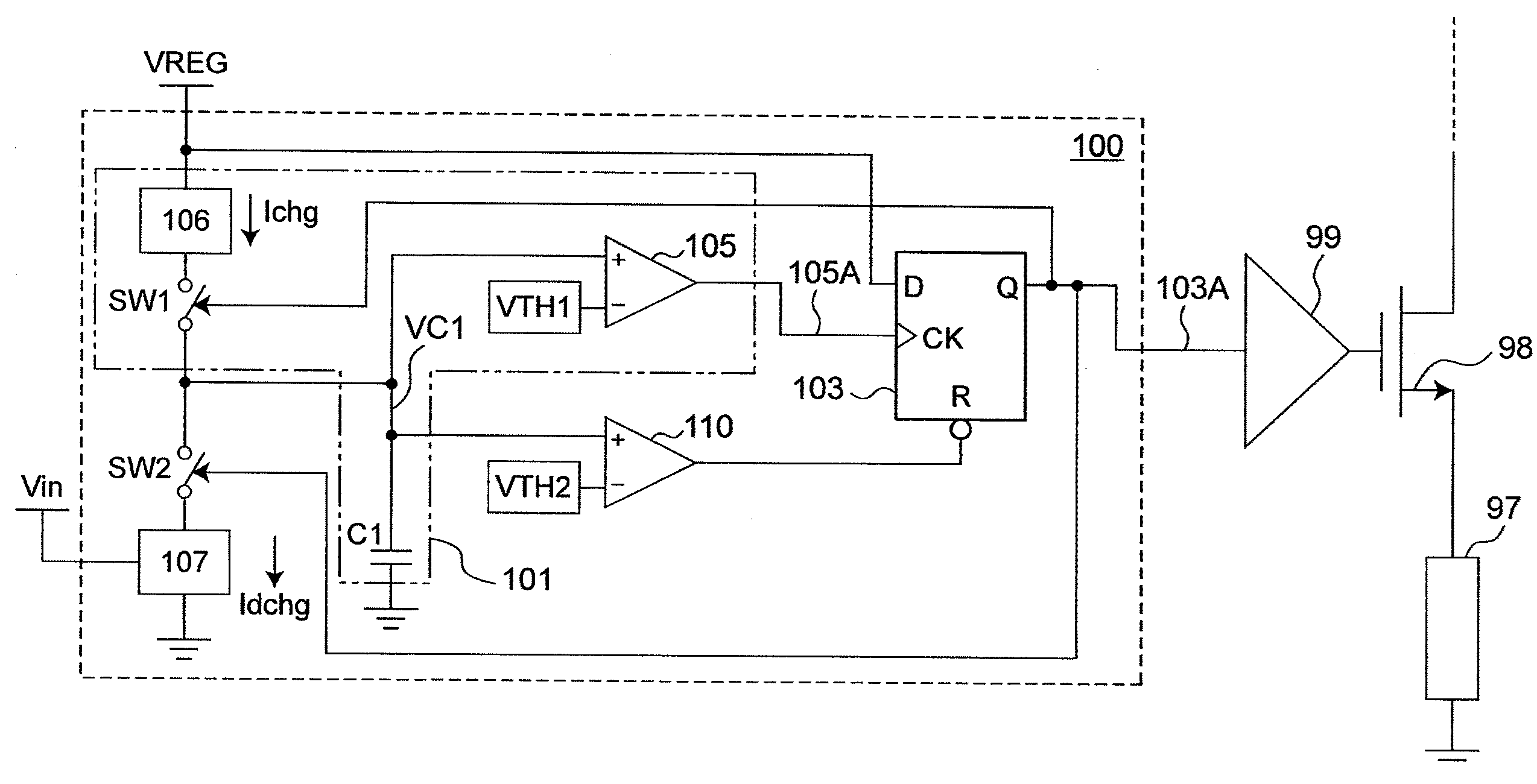
[0030]Referring to FIG. 2, a first embodiment of an On-Off Timer according to the present invention is shown.
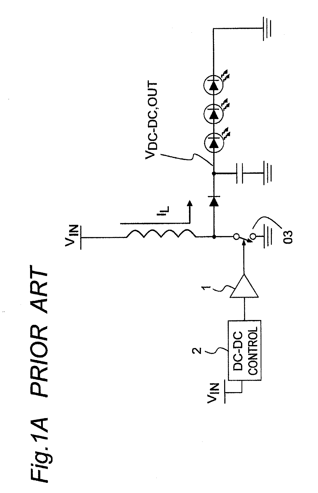
[0031]As shown in FIG. 2, the On-Off Timer 100 outputs to a driver block 99, which drives an exemplary output stage comprising an NMOS output power transistor 98 and sense resistor 97 coupled to the emitter terminal of the NMOS output power transistor 98. On-Off Timer 100 may be implemented within the DC-DC control 2 of FIG. 1A.
[0032]The On-Off Timer 100 comprises an Off-Timer 101, an On-Timer 102 and a flip-flop 103 which generates a first level signal and a second level signal from its output. The first level signal and the second level signal can be a LOW level signal and a HIGH level signal, or vice versa. As the name suggests, flip-flop 103 may be of any known types of flip-flops, such as the D flip-flop, SR flip-flip or the JK flip-flop. DC voltage levels VREG and Vin are inputted to provide bias voltage and input voltage respectively. VREG is a constant voltage that ma...
second embodiment
[0059]Referring to FIG. 5A and FIG. 5B, a second embodiment of an On-Off Timer according to the present invention is shown. The Off-timer and On-timer for the second embodiment are as highlighted in FIG. 5A and FIG. 5B respectively.
[0060]Here, it is designed to accept an ENABLE signal, for extra control. The ENABLE signal may be generated from a CPU or initiated by the user. An AND gate 120 is incorporated into the circuit, with its input being the ENABLE signal and the output of comparator 110. With the ENABLE signal, the output Q of D flip-flop 103 can be made low independent of the voltage at VC1.
[0061]During initial condition, VC1=0; the ENABLE signal is logic LOW, causing the D flip-flop 103 to reset, that is, output Q goes to logic LOW. This further results in NMOS output power transistor 98 being turned off. When ENABLE signal goes logic HIGH, output Q of D flip-flop 103 remains logic LOW, corresponding to the start of the timing duration of the Off-Timer 101. As described ea...
third embodiment
[0063]Referring to FIG. 6A and FIG. 6B, a third embodiment of an On-Off-Timer 101 according to the present invention is shown. The Off-timer and On-timer for the third embodiment are as highlighted in FIG. 6A and FIG. 6B respectively.
[0064]In the present embodiment, additional circuit elements have been added. These additional elements are: Logic Control 130, switch 131, comparator 132, and NOT gate 133. Switch 131 may be in the form of any known solid-state switches. For the purpose of explanation, an exemplary NMOS switch is used as switch 131, as shown in FIG. 3D.
[0065]Comparator 132 may be external or internal within the circuit. For the purpose of explanation, an exemplary implementation of comparator 132 external to the On-Off Timer 100 is used.
[0066]The purpose of the comparator 132 is to detect when the voltage VS is equal to a reference DC voltage VS—REF, where this would imply that the output current has reached the maximum threshold output current allowable (represented b...
PUM
 Abstract
Description
Claims
Application Information