Layout for antenna loops having both functions of capacitance induction and electromagnetic induction

a technology of capacitance induction and electromagnetic induction, which is applied in the direction of loop antennas, resistance/reactance/impedence, instruments, etc., can solve the problems of inconvenient use, inability to directly use fingers to write or paint on electric devices, and inability to precisely detect the position of use's fingers, etc., to achieve the effect of reducing the cost reducing the process of fabricating this layout, and low cos

Active Publication Date: 2011-09-22
WACOM CO LTD
View PDF13 Cites 44 Cited by
  • Summary
  • Abstract
  • Description
  • Claims
  • Application Information

AI Technical Summary

Benefits of technology

[0008]The first switch assembly is deposed between the first connecting terminal and the first connecting section and between the second connecting terminal and the first connecting section for controlling the first antenna section, the second antenna section and the first connecting section to be electrically connected with each for forming a first antenna loop. The ground switch assembly is connected with the second signal terminal of the second antenna section for controlling the second signal terminal to electrically connect with the ground and for controlling the first antenna section, the second antenna section, and the first connecting section to connect with the ground. The layout is separated into the first antenna section, the second antenna and the first connecting section by the first switch assembly, and the first switch assembly controls the first antenna section, the second antenna and the first connecting section to connect with each other and to separate from each other. Therefore, the first switch assembly controls the first antenna loop to form and to separate from three sections. There are several first geometric structures arranged in the first antenna section and there are many second geometric structures arranged in the second antenna section. Therefore, when the first antenna section, the second antenna and the first connecting section are separated from each other by the first switch assembly, the first antenna section and the second antenna section can be respectively uses as a series of the capacitance induction elements for capacitance induction. In consequence of this structure, capacitance detection elements are integrated with the antenna loops into an antenna loop and they are formed on the same substrate. Therefore, the layout unlike the conventional input inputting device having both functions of capacitance induction and electromagnetic induction to form the capacitance detection elements and the antenna loops on different substrates. This layout can be formed on the substrate by printing or a mask. Therefore, the cost of fabricating this layout is reduced and the process for fabricating this layout is simplified. Furthermore, the capacitance induction elements will not shield the antenna loops from the electromagnetic signals anymore because the capacitance induction elements are parts of the antenna loops. Therefore, this layout for antenna loops can have both functions of capacitance induction and electromagnetic induction and have the characteristics of low cost and simple fabricating process.
[0009]Therefore, the effect achieved with the present invention is to provide a layout for antenna loops having both functions of capacitance induction and electromagnetic induction. In this layout, the capacitance detection elements are integrated with the antenna loops for avoiding the situation that the capacitance detection elements shields the antenna loops from the electromagnetic signals. Furthermore, the cost of this layout can be reduced and the process for fabricating this layout can be simplified.

Problems solved by technology

Therefore, it is inconvenient to the user.
Although a user can use his fingers to hand write on the electric devices applying to the capacitance induction technology and it is convenient to the user, but the electric devices can not detect the position of the use's fingers precisely.
Therefore, the user can not directly use his fingers to write or paint on the electric device and it needs a special pointing device for hand writing.
Although the situation that the electromagnetic signals are shielded by the capacitance induction elements (touch elements) is improved by this method, but the shielding can not be removed completely.
Furthermore, it is difficult to form silts on small capacitance induction elements (touch elements) and the process for fabricating these slits is complicated.
Therefore, it has a need of more cost and time for forming these capacitance induction elements (touch elements).
Besides, the cost for fabricating these capacitance induction elements (touch elements) is increased because the capacitance induction elements (touch elements) and the antenna loops are respectively formed on different substrates for forming a touch board and an antenna loops board.

Method used


Image

  • Layout for antenna loops having both functions of capacitance induction and electromagnetic induction
  • Layout for antenna loops having both functions of capacitance induction and electromagnetic induction
  • Layout for antenna loops having both functions of capacitance induction and electromagnetic induction

Examples


Embodiment Construction

[0019]Although the present invention will be described in accordance with following embodiments, one of ordinary skill in the art will readily recognize that there could be variations to the embodiments and those variations would be within the spirit and scope of the present invention. Accordingly, many modifications may be made by one of ordinary skill in the art without departing from the spirit and scope of the appended claims.

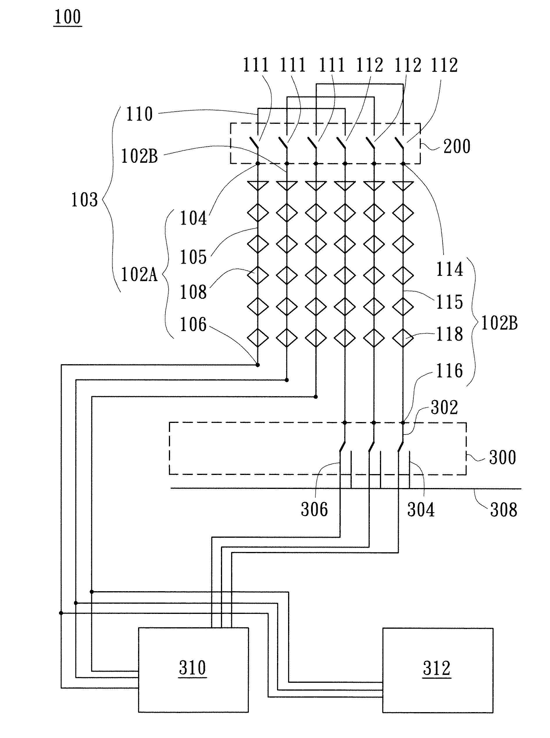
[0020]Referring to FIG. 2A, it is a plane view form diagram illustrating a layout 100 for antenna loops having both functions of capacitance induction and electromagnetic induction in accordance with one embodiment of the present invention. The layout 100 is distributed in X-direction of two-dimensional coordinates. The layout 100 for antenna loops having both functions of capacitance induction and electromagnetic induction comprises first antenna sections 102A, second antenna sections 102B, first connecting sections 110, a first switch assembly 200, a grou...


PUM


Abstract

The present invention relates to a layout for antenna loops having both functions of capacitance induction and electromagnetic induction, and particularly relates to the layout for antenna loops having both functions of capacitance induction and electromagnetic induction, wherein the capacitance detection elements are integrated with the antenna loops. In this layout for antenna loops, each of the antenna loops therein is separated into three sections, and there are several geometric structures fabricated in two of these sections. These geometric structures are capacitance detection elements. Therefore, the two sections are directly fabricated to be the capacitance detection elements because of these geometric structures. By this way, the antenna loops can be integrated with the capacitance detection elements and the capacitance detection elements do not prevent the antenna loops from receiving the electromagnetic signals.

Description

FIELD OF THE INVENTION[0001]The present invention relates to a layout for antenna loops having both functions of capacitance induction and electromagnetic induction, and particularly relates to the layout for antenna loops having both functions of capacitance induction and electromagnetic induction, wherein the capacitance detection elements are integrated with the antenna loops.BACKGROUND OF THE INVENTION[0002]Because the hand writing technology is applied to various kinds of electric devices popularly, for example computer, tablet, cell phone or PDA, the capacitance induction technology and the electromagnetic induction technology are applied to these devices popularly. In the electric devices applying the electromagnetic induction technology, there are some antenna loops applied to electromagnetic inducing with a special pointing device, for example a special pen, for hand writing. In the electric devices applying the capacitance induction technology, a user can directly use his ...

Claims


Application Information

Patent Timeline
Patent Type & Authority Applications(United States)
IPC IPC(8): H01Q21/00H01Q7/00G01R27/26G01R27/28
CPCG06F3/044G06F3/046H01Q21/061H01Q1/44G06F2203/04106G06F3/0445G06F3/0446
Inventor CHEN, WEI-CHOUCHEN, KE-WEIHUANG, CHIA-TE
Owner WACOM CO LTD
Why Eureka
Try Eureka