
Storage subsystem

a subsystem and storage technology, applied in the field of storage subsystems, can solve the problems of hdd data being overwritten, configuration subsystems being unable to recover data, and hdd data being impossible to recover, so as to achieve the effect of lessening load

Inactive Publication Date: 2011-09-29
HITACHI LTD
View PDF14 Cites 68 Cited by
  • Summary
  • Abstract
  • Description
  • Claims
  • Application Information

AI Technical Summary

Benefits of technology

[0017]According to the present invention, when updating data in a nonvolatile semiconduct...

Problems solved by technology

However, if malfunctions should occur in more than a predetermined number of memory drives, it becomes impossible to recover the data even in a RAID-configured subsystem.
However, when updating HDD data, the HDD data may be overwritten.
For this reason, there is the possibility of the old parity stored in the HDD being lost as a result of the over...

Method used


Image

  • Storage subsystem
  • Storage subsystem
  • Storage subsystem

Examples


embodiment 1

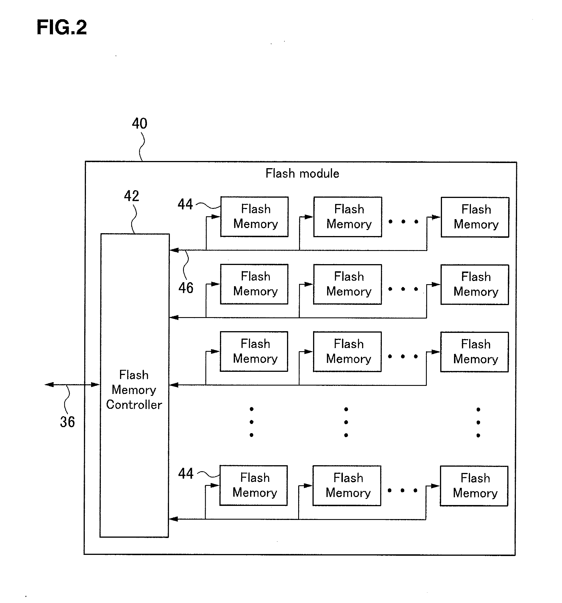
[0054]This embodiment is configured such that during a random write, the main processor, which controls the cache, creates an XOR write command at the time the update data is written to the flash module, and transfers the created XOR write command to the flash memory controller that controls the flash memory, the flash memory controller parses the XOR write command, reads out the old parity from the parity-storage flash memory, creates a new parity by carrying out an exclusive OR operation using the read-out old parity and the old data and new data added to the XOR write command, and stores the created new parity in the parity-storage flash memory.

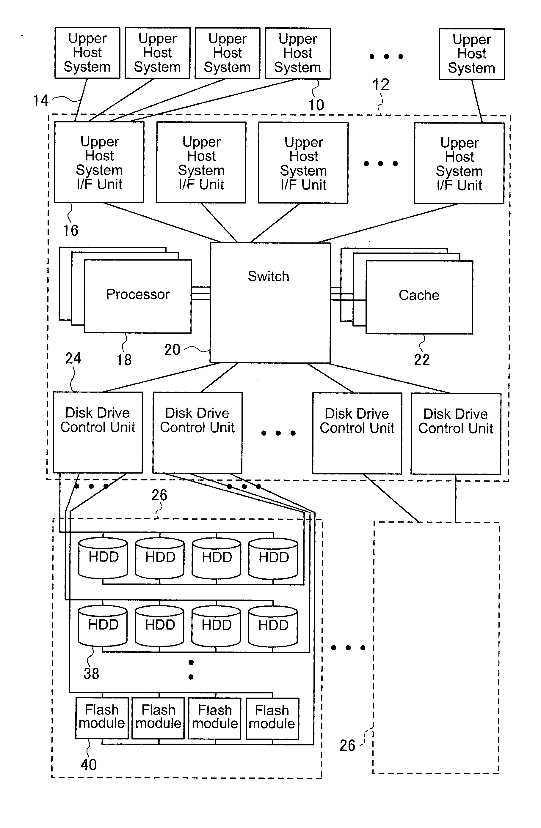
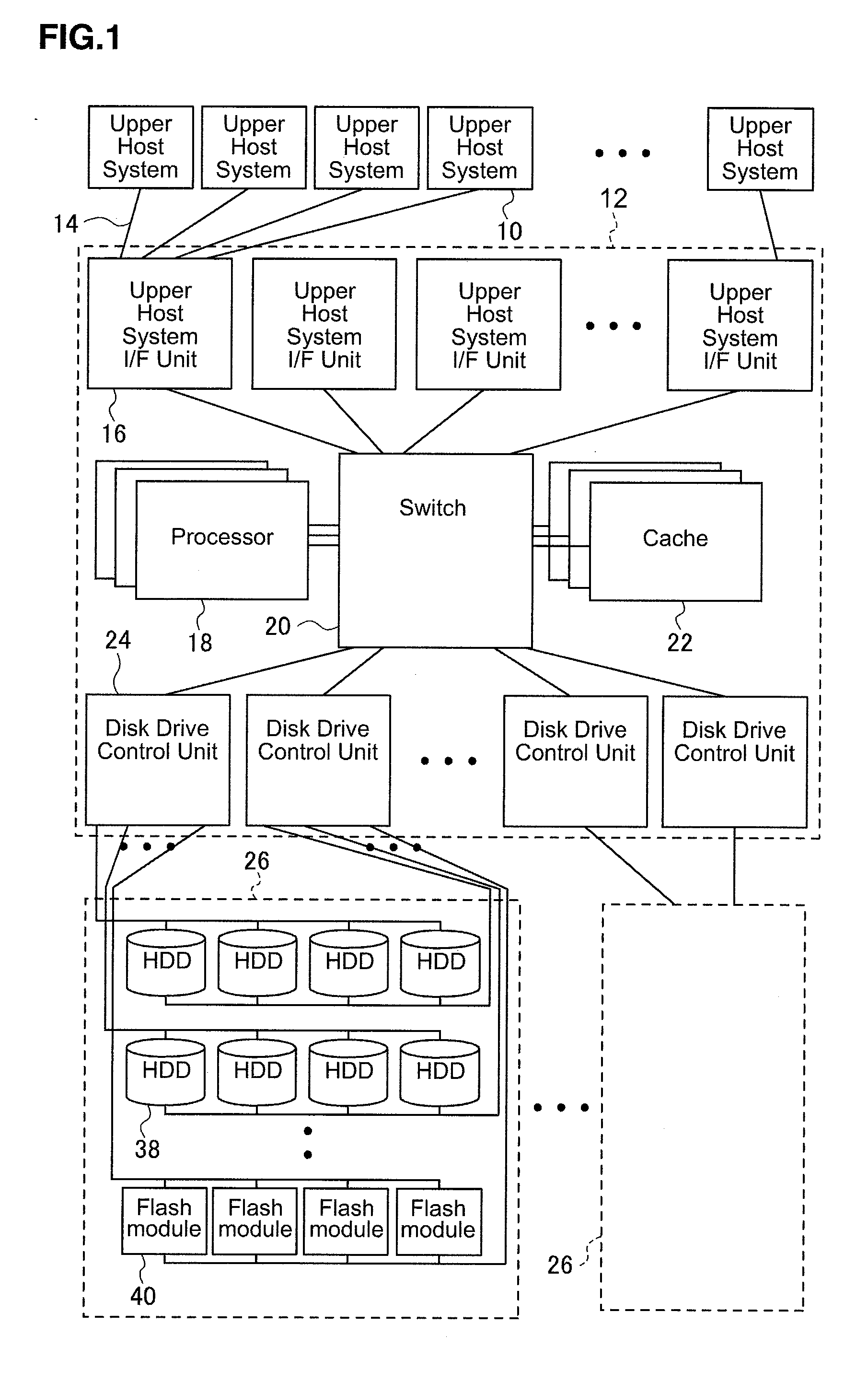
[0055]The first embodiment of the present invention will be explained below based on the drawings. FIG. 1 is a block diagram of a storage system showing the first embodiment of the present invention.

[0056]In FIG. 1, the storage system comprises a plurality of upper host systems 10 and a storage subsystem 12, and each upper host system 10 i...

embodiment 2

[0106]Next, a second embodiment of the present invention will be explained in accordance with FIG. 13. This embodiment is configured such that a NV-RAM (Non Volatile Random Access Memory) 110 is disposed as a status recording memory in the flash memory controller 42 and a conversion table for converting a logical address to a physical address is stored in the RAM 50, the contents of the conversion table are updated in a process in which the microprocessor 48 carries out input / output processing to / from the respective flash modules 40 and the processing status is also sequentially recorded in the NV-RAM 110, and the recorded content is transferred to the main processor 18 by way of the host interface 54 making it possible for processing to commence from the place instructed in instruction information from the main processor 18 even when a malfunction occurs part way through the processing. The remainder of the configuration is the same as that of the first embodiment.

[0107]Next, t...


PUM


Abstract

Processing in accordance with the updating of data is carried out distributively by a control unit that controls a cache memory and by a memory controller that controls a nonvolatile semiconductor memory. When updating flash memory data, a main processor creates an XOR write command and transfers the same to a flash memory controller, a microprocessor of the flash memory controller parses the XOR write command, reads out an old parity from a page of a user area in the flash memory, creates a new parity by carrying out an exclusive OR operation using the read-out old parity, “b” data, which is the old data, and “d” data, which is the new data, and stores the created new parity in a page of a renewal area in a flash memory for storing parity.

Description

TECHNICAL FIELD[0001]The present invention relates to a storage subsystem mounted with nonvolatile semiconductor memory such as flash memory in a storage apparatus.BACKGROUND ART[0002]In recent years, attention has focused on flash memory, a typical nonvolatile semiconductor memory, for storage devices. Because a flash memory does not have a drive portion like a magnetic storage device typified by an HDD (Hard Disk Drive), it features lower power consumption than a HDD. A storage device that uses a memory drive mounted with a plurality of flash memories instead of a HDD has been proposed as an external storage device (Refer to Patent Document 1).[0003]Meanwhile, a storage subsystem must be stable, and as such, employs a configuration with duplexed components that enables processing to be carried out even when a malfunction occurs in a portion of the components. For example, in order to heighten data integrity and throughput, RAID (Redundant Array of Inexpensive Disks) technology is ...

Claims


Application Information

Patent Timeline
IPC IPC(8): G06F12/00
CPCG06F3/0613G06F3/0659G06F3/0688G06F3/0679G06F2211/1054G06F3/0604G06F3/0658G06F11/108
Inventor KITAHARA, JUNTAKADA, MASANORISUGIMOTO, SADAHIRO
Owner HITACHI LTD
Learn More