Display device and electronic appliance

a technology of electronic appliances and display devices, applied in the field of display devices and electronic appliances, can solve problems such as damage to uniform screens, and achieve the effects of reducing capacitance values, improving bootstrap gain, and improving bootstrap gain

Inactive Publication Date: 2011-10-06
SONY CORP
View PDF7 Cites 3 Cited by
  • Summary
  • Abstract
  • Description
  • Claims
  • Application Information

AI Technical Summary

Benefits of technology

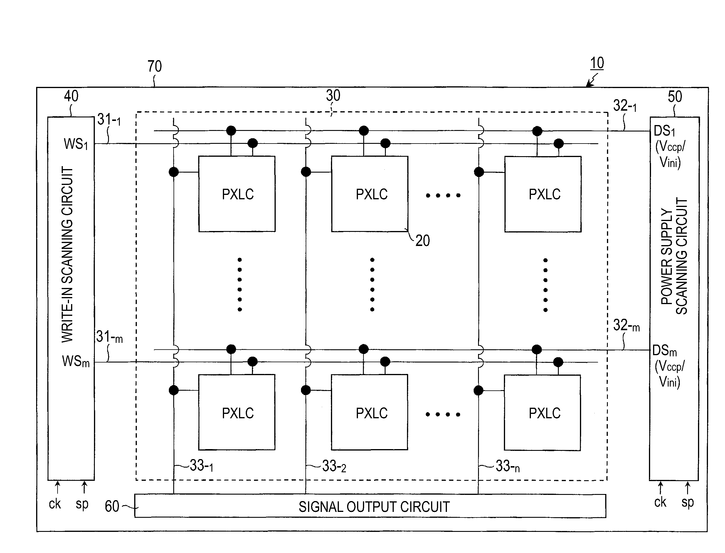
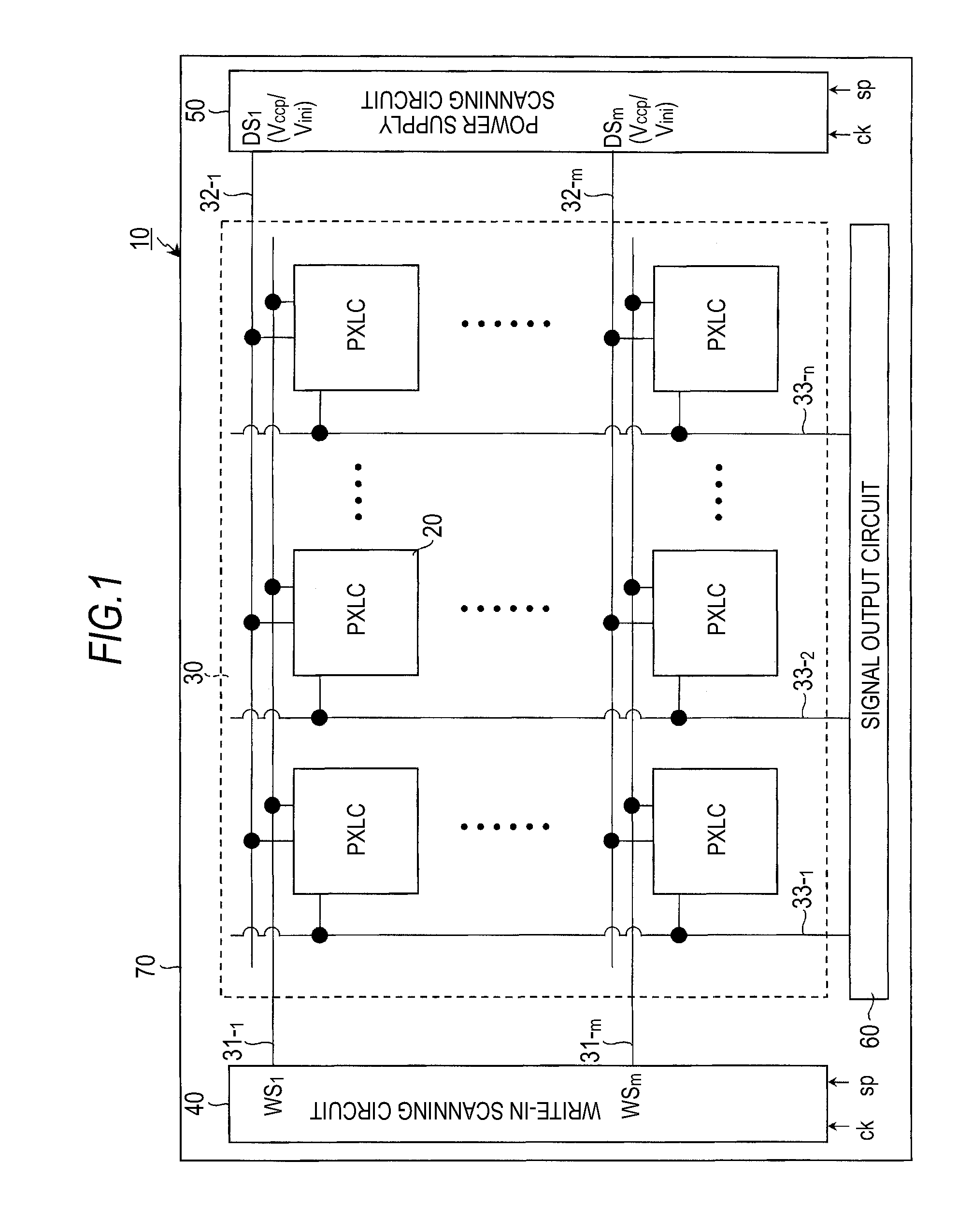
[0012]Accordingly, it is desirable to provide a display device which can improve the bootstrap gain by reducing the capacitance value between the gate and source of the driving transistor and obtain a good-quality display image without damaging the uniformity of the screen, and an electronic appliance having the display device.
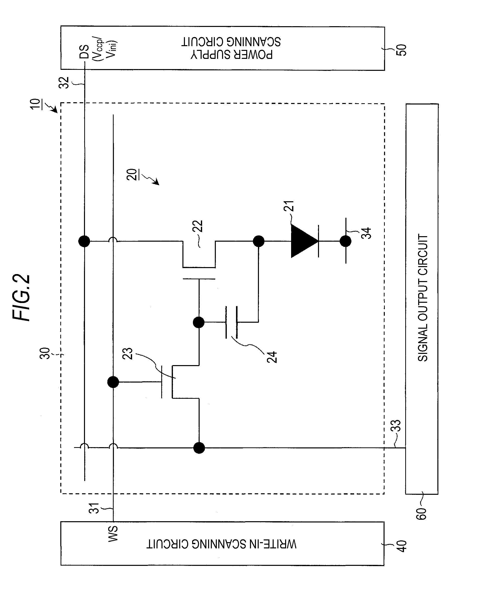
[0014]In the driving transistor having the sandwich gate structure, if the anode electrode of the electro-optical component does not exist in a region that is opposite to one of the two gate electrodes, that is, a so-called back gate electrode, the back gate electrode is opposite to the cathode electrode. Accordingly, a parasitic capacitance is formed between the back gate electrode and the cathode electrode. This parasitic capacitance acts in a direction in which the capacitance value of the parasitic capacitance that is parasitic on the gate electrode of the driving transistor is increased. That is, as the anode electrode of the electro-optical component is opposite to at least a portion of the back gate electrode, the parasitic capacitance is formed between the opposite regions of both the electrodes. This parasitic capacitance acts in a direction in which the parasitic capacitance that is parasitic on the gate electrode of the driving transistor, particularly, the capacitance value between the gate and the source of the driving transistor, is reduced. Accordingly, the bootstrap gain can be improved.
[0015]According to the embodiment of the invention, since the bootstrap gain is improved by reducing the capacitance value between the gate and the source of the driving transistor, a good-quality display image can be obtained without damaging the uniformity of the screen.

Problems solved by technology

As a result, the uniformity of a screen is damaged.

Method used


Image

  • Display device and electronic appliance
  • Display device and electronic appliance
  • Display device and electronic appliance

Examples


examples

[0152]The pixel structure according to an example having the driving transistor 22 of the sandwich gate structure will be described using FIG. 18. FIG. 18 is a cross-sectional diagram illustrating a pixel structure according to an embodiment having a driving transistor 22 of a sandwich gate structure. In the drawing, the same reference numerals are used for the equivalent portions to those in FIG. 16.

[0153]The driving transistor 22 has the same sandwich gate structure as the case of the pixel structure according to the reference example as described above. That is, the driving transistor 22 has a structure in which the channel region 225 is sandwiched between the first gate electrode 221 arrange on the substrate side with respect to the channel region 225 and the second gate electrode 226 arranged on the opposite side as the back gate electrode. Also, the driving transistor 22 adopts an LDD structure in which low-density impurity regions having a density that is lower than that of t...


PUM


Abstract

A display device includes: a plurality of arranged pixels, each of which includes an electro-optical component, a write-in transistor writing an image signal in a pixel, a maintenance capacity maintaining the image signal written by the write-in transistor, and a driving transistor driving the electro-optical component based on the image signal maintained by the maintenance capacity; wherein the driving transistor has a sandwich gate structure in which a channel region is sandwiched between two gate electrodes, and the electro-optical component is formed so that at least a portion of one of the two gate electrodes and an anode electrode are opposite to each other.

Description

BACKGROUND OF THE INVENTION[0001]1. Field of Invention[0002]The invention relates to a display device and an electronic appliance, and more particularly to a display device in which pixels including electro-optical components are two-dimensionally (2D) arranged in the form of a matrix and an electronic appliance having the display device.[0003]2. Description of the Related Art[0004]Recently, in the field of display devices that perform image display, plane-type (flat panel type) display devices in which pixels (pixel circuits) are arranged in the form of a matrix have been rapidly spread. As a kind of plane type display device, there is a display device that uses a so-called current driving type electro-optical component, in which luminance is changed according to a current value that flows in the device, as a light-emitting device of a pixel. As a current driving type electro-optical component, an organic electroluminescence (EL) device is known, which has a phenomenon of emitting ...

Claims


Application Information

Patent Timeline
Patent Type & Authority Applications(United States)
IPC IPC(8): G06F3/038
CPCG09G3/3233G09G2300/0819G09G2320/043G09G2300/0866G09G2300/0842
Inventor OMOTO, KEISUKE
Owner SONY CORP
Why Eureka
Try Eureka