Semiconductor device and decoding method thereof

Active Publication Date: 2011-10-06
SAMSUNG ELECTRONICS CO LTD
View PDF5 Cites 37 Cited by
  • Summary
  • Abstract
  • Description
  • Claims
  • Application Information

AI Technical Summary

Benefits of technology

[0006]At least one embodiment of the inventive concept provides a semiconductor device, which may improve bit error rate (BER) per

Problems solved by technology

Data that is received during one of these communications may contain an error.
However, conventional e

Method used


Image

  • Semiconductor device and decoding method thereof
  • Semiconductor device and decoding method thereof
  • Semiconductor device and decoding method thereof

Examples


Embodiment Construction

[0036]The inventive concept will now be described more fully with reference to the accompanying drawings, in which exemplary embodiments thereof are illustrated. In the drawings, like reference numerals denote like elements.

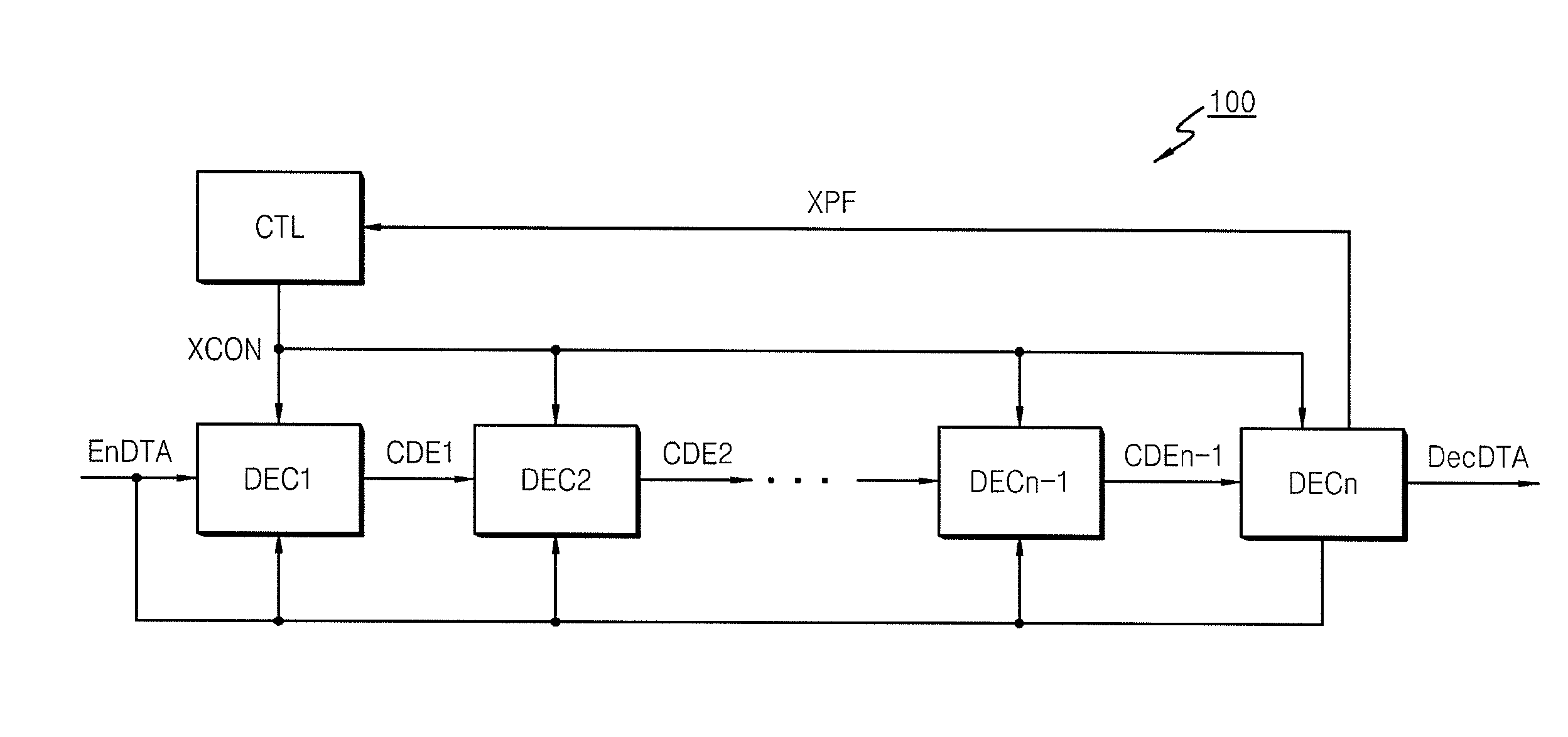
[0037]FIG. 1 illustrates a decoding unit 100 included in an error control coding (ECC) block, according to an exemplary embodiment of the inventive concept. Referring to FIG. 1, the decoding unit 100 includes a plurality of first decoders DEC1, DEC2, . . . , and DECn−1, a second decoder DECn, and a controller CTL.

[0038]The first decoders DEC1, DEC2, . . . , and DECn−1 are sequentially connected to each other such that an output of a previous decoder is fed to a next decoder. The first decoders DEC1, DEC2, . . . , and DECn−1 may perform decoding operations based on decoding results of a previous decoder. For example, the decoder DEC2 decodes a code CDE1 decoded by the decoder DEC1 and outputs a code CDE2. However, the decoder DEC1, which is the first one of the fi...


PUM


Abstract

An error control coding (ECC) circuit includes a first decoder, a second decoder, and a controller. The first decoder receives encoded data comprising a first parity and a second parity. The first decoder decodes the encoded data to a first code by using the first parity. The second decoder is connected to the first decoder. The second decoder is configured to decode the encoded data when the first decoder is deactivated and decode the first code using the second parity when the first decoder is deactivated. The controller transmits a control signal to the first decoder and the second decoder to control the first decoder and the second decoder.

Description

CROSS-REFERENCE TO RELATED APPLICATION[0001]This application priority to Korean Patent Application No. 10-2010-0030507, filed on Apr. 2, 2010, in the Korean Intellectual Property Office, the disclosure of which is incorporated by reference in its entirety herein.BACKGROUND[0002]1. Technical Field[0003]Exemplary embodiments of the inventive concept relate to a semiconductor device and a decoding method thereof, and more particularly, to a semiconductor device, which may improve the performance of error control coding (ECC) and reduce power consumption, and a decoding method of the semiconductor device.[0004]2. Discussion of Related Art[0005]Electronic devices may include one or more semiconductor devices. High-speed communication may be performed internally between elements within a semiconductor device or externally among the semiconductor devices themselves. Data that is received during one of these communications may contain an error. Thus, some form of error detection and correct...

Claims


Application Information

Patent Timeline
IPC IPC(8): G06F11/08
CPCG06F11/1048H03M13/00
Inventor KIM, YONG-JUNEKONG, JUN-JINLEE, YOUNG-HWANKIM, JAE-HONG
Owner SAMSUNG ELECTRONICS CO LTD
Why Eureka
Try Eureka