Electrophoretic display device and electronic apparatus

a display device and display device technology, applied in static indicating devices, non-linear optics, instruments, etc., can solve problems such as difficulty in performing full-color displays, and achieve excellent color displays

Inactive Publication Date: 2011-10-13
SEIKO EPSON CORP
View PDF29 Cites 13 Cited by
  • Summary
  • Abstract
  • Description
  • Claims
  • Application Information

AI Technical Summary

Benefits of technology

[0009]An advantage of some aspects of the invention is that an electrophoretic display device and an electronic apparatus are provided which are able to control at least one or all three of brightness, saturation, and hue by controlling movement of electrophoretic particles and to perform an excellent color display.

Problems solved by technology

There are issues with the controllability of brightness and saturation in one sub pixel in order to realize a color electrophoretic display device, and it is difficult to perform a full-color display.
A pixel layout and form which resolves this is also an issue.

Method used


Image

  • Electrophoretic display device and electronic apparatus
  • Electrophoretic display device and electronic apparatus
  • Electrophoretic display device and electronic apparatus

Examples


first embodiment

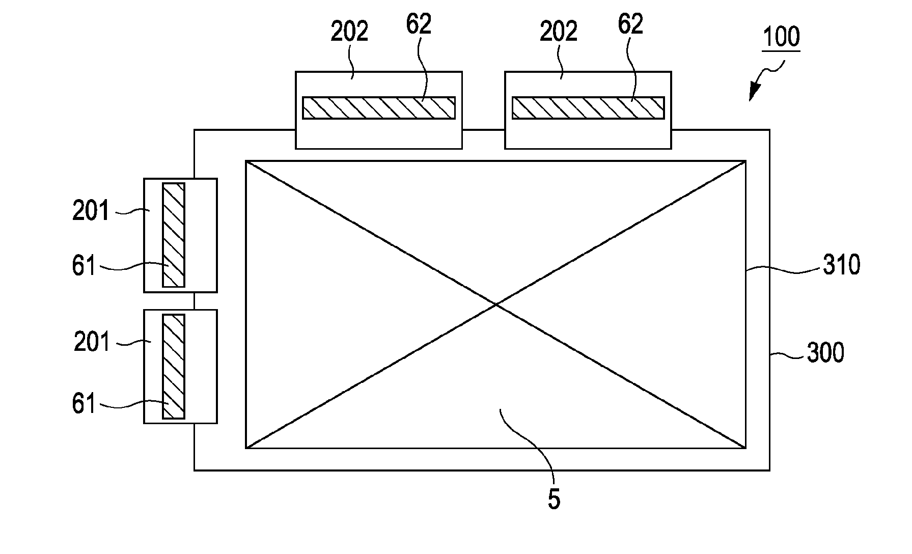
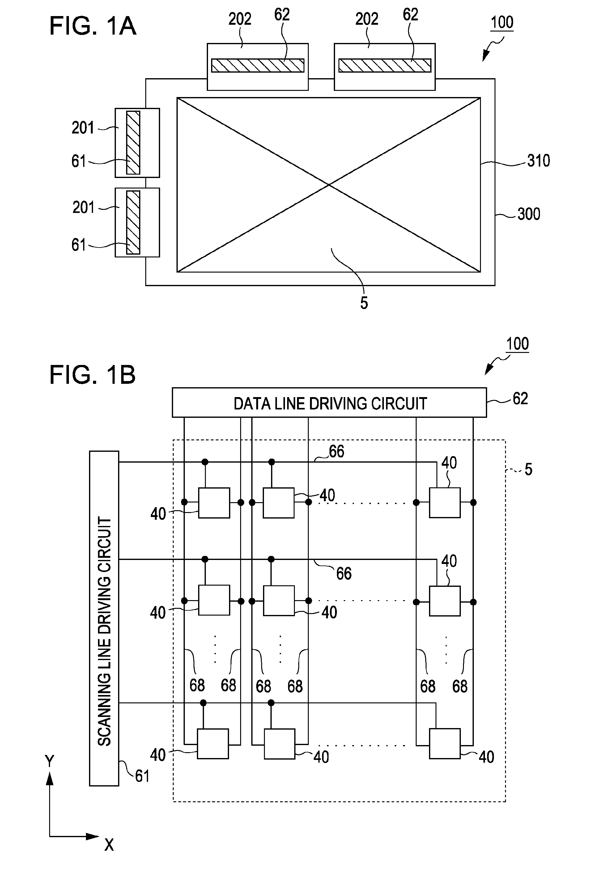
[0100]FIG. 1A is a planar diagram illustrating an overall configuration of an electrophoretic display device 100.

[0101]As shown in FIG. 1A, in the electrophoretic display device 100 of the embodiment, an element substrate 300 has larger planar dimensions than that of an opposing substrate 310, and on the element substrate 300 which protrudes to the outside more than the opposing substrate 310, two scanning line driving circuits 61 and two data line driving circuits 62 are COF (Chip On Film) mounted (or TAB (Tape Automated Bonding) mounted) on flexible substrates 201 and 202 which are for connection to external devices. Then, the flexible substrates 201, where the scanning line driving circuits 61 are mounted, are mounted in terminal formation regions formed on a side edge portion along one short side of the element substrate 300 via ACP (anisotropic conductive paste), ACF (anisotropic conductive film), or the like. Here, the element substrate 300 is configured of the first substrate...

second embodiment

[0214]Next, an electrophoretic display device according to a second embodiment will be described. Below, the parts which differ from the first embodiment will be described. The other parts are similar to the first embodiment.

[0215]FIG. 17 is a planar diagram illustrating a schematic configuration of one pixel according to the second embodiment, and FIG. 18 is a cross-sectional diagram along a line XVIII-XVIII of FIG. 17.

[0216]The electrophoretic display device according to the second embodiment is provided with the plurality of first pixel electrodes 35A, the plurality of second pixel electrodes 35B, the first connection electrode 44A, the second connection electrode 44B, the selection transistor TR1, and the selection transistor TR2 in one pixel in the same manner as the previous embodiment, but in the embodiment, the further provision of drain connection electrodes 45A and 45B and a interlayer insulating film 42C described later is different.

[0217]As shown in FIG. 17, the drain co...

third embodiment

[0237]Next, an electrophoretic display device according to a third embodiment will be described. Below, the parts which differ from the first embodiment will be described. The other parts are similar to the first embodiment.

[0238]FIG. 22A is a planar diagram schematically illustrating a state of a pixel arrangement in a display region of an electrophoretic display device according to the third embodiment and FIG. 22B is a planar diagram illustrating a configuration of one pixel. FIG. 23 is a planar diagram illustrating a specific configuration example of one pixel.

[0239]As shown in FIG. 22A, in the electrophoretic display device according to the embodiment, the pixel 40A where the pixel electrodes 35A and 35B are arranged in the first layout L1 and the pixel 40B where the pixel electrodes 35A and 35B are arranged in a second layout L2 are mixed in a matrix formation in the display region. That is, in both the row direction and the column direction, the pixel 40A arranged in the firs...


PUM

PropertyMeasurementUnit
chargeaaaaaaaaaa
negative chargeaaaaaaaaaa
transparencyaaaaaaaaaa

Abstract

Provided is an electrophoretic display device including: a first substrate; a second substrate; an electrophoretic layer which is arranged between the first substrate and the second substrate and has at least a dispersion medium and particles mixed in the dispersion medium; a plurality of first electrodes which is formed in an island shape on the electrophoretic layer side of the first substrate and is provided for each pixel; and a second electrode which is formed on the electrophoretic layer side of the second substrate with an area wider than that of the first pixel electrode. Gradation is controlled using an area of the particles which are visually recognized when the electrophoretic layer is viewed from the second electrode side.

Description

CROSS-REFERENCE TO RELATED APPLICATION[0001]This application is based on and claims priority from Japanese Patent Application No. 2010-091370, filed on Apr. 12, 2010, and Japanese Patent Application No. 2011-056717, filed on Mar. 15, 2011, the contents of which are incorporated herein by reference.BACKGROUND[0002]1. Technical Field[0003]The present invention relates to an electrophoretic display device and an electronic apparatus.[0004]2. Related Art[0005]In recent years, electrophoretic display devices have come to be used as a display portion such as electronic paper. An electrophoretic display device has a configuration which has an electrophoretic dispersion liquid where a plurality of electrophoretic particles is dispersed in a liquid-phase dispersion medium (dispersion medium). The electrophoretic display device is a device used for display where the distribution state of the electrophoretic particles changes due to the application of an electric field and the optical properti...

Claims


Application Information

Patent Timeline
Patent Type & Authority Applications(United States)
IPC IPC(8): G09G3/34G02F1/1676
CPCG09G3/344G09G2300/0452G02F2001/1676G02F1/1362G09G2300/0809G02F1/1676
Inventor SATO, TAKASHI
Owner SEIKO EPSON CORP
Why Eureka
Try Eureka