

Semiconductor device and manufacturing method thereof
a technology of semiconductor devices and semiconductors, applied in the direction of semiconductor devices, basic electric elements, electrical equipment, etc., can solve the problems of reducing production yield, difficult to use flexible substrates made of plastics or something with a low melting point, and crystalline silicon application, so as to reduce contact resistance
- Summary
- Abstract
- Description
- Claims
- Application Information
AI Technical Summary
Benefits of technology
Problems solved by technology
Method used
Image

Examples
exemplary embodiment 1
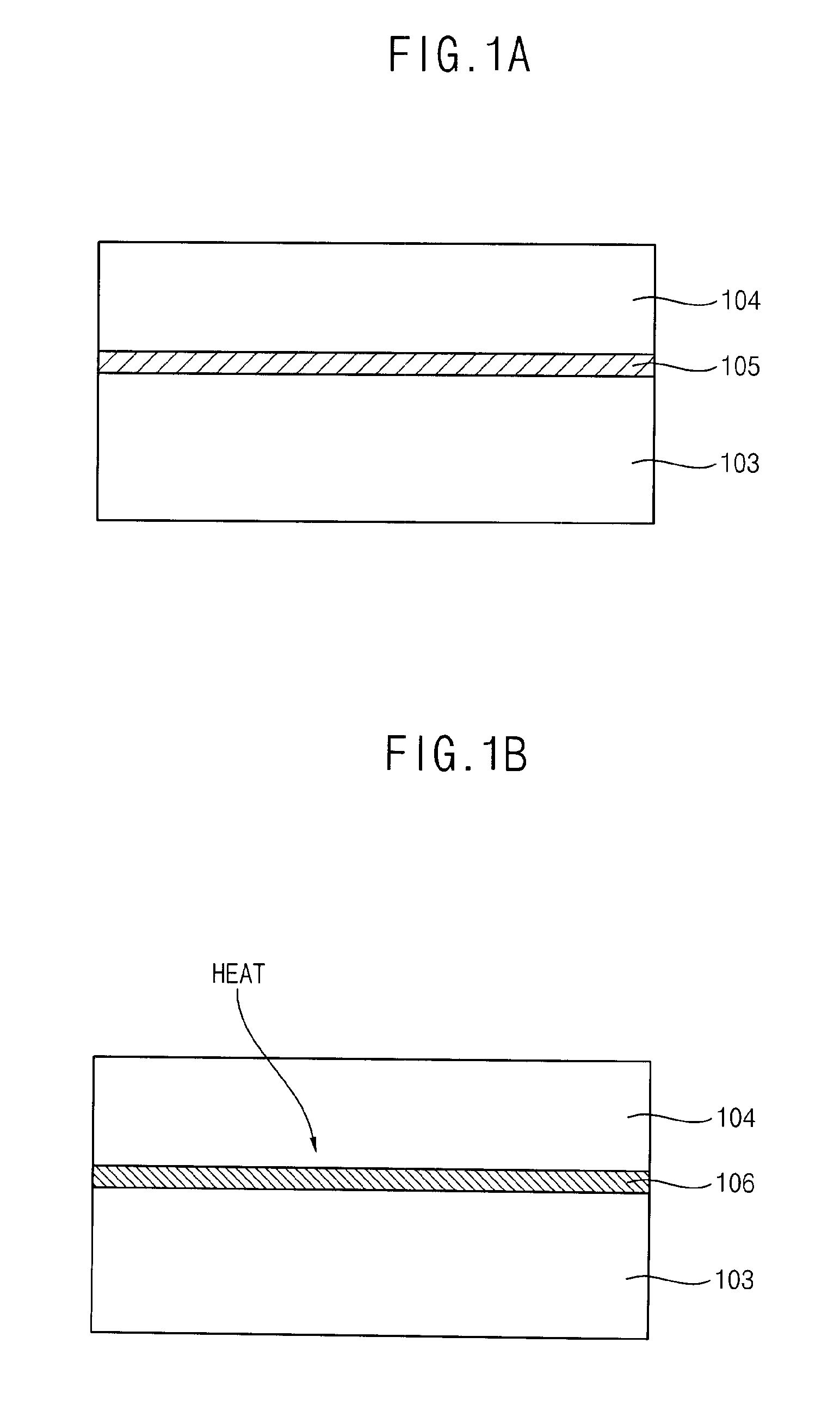
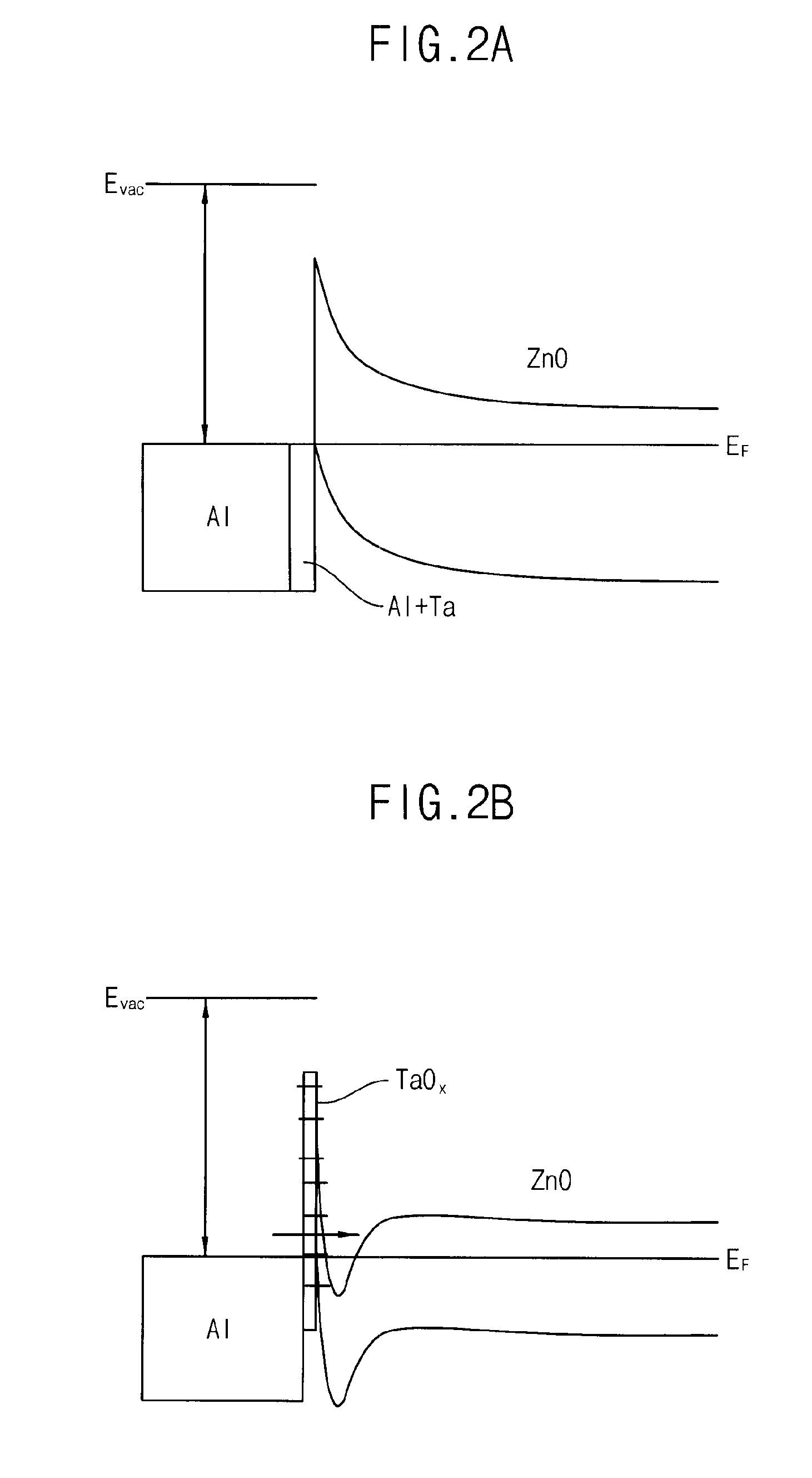
[0028]FIG. 1A shows a contact layer 105 placed between a semiconductor layer 103 and a wiring 104. In this exemplary embodiment of the invention, a low resistant contact layer 106 (depicted in FIG. 1B) is formed, which may improve the crystallinity of the semiconductor layer 103.
[0029]The semiconductor layer 103 in one exemplary embodiment of the invention is highly doped. For example, semiconductor layer 103 may include n+Si on amorphous Si, which may overcome a Schottky barrier to provide a low resistant contact layer between semiconductor layer 103 and wiring 104. This example utilizes the physical principle that contact resistance depends particularly on doping concentration, as described in Equation 1 below.
Rc=Aexp[(2ΦBn(N / m*∈s)1 / 2) / { cot h(q / 2kT(N / m*∈s)1 / 2)}] (1)
[0030]Rc is the contact resistance, N is the doping concentration, ΦBn is the barrier height in an energy band diagram, and T is temperature.
[0031]However, a highly doped oxide semiconductor layer may not be a low r...
exemplary embodiment 2
[0038]In this exemplary embodiment of the invention, a nitride semiconductor layer 103 including a low resistant contact layer 106 is formed and crystallinity may be improved. Exemplary Embodiment 2 is similar to Exemplary Embodiment 1 except for the semiconductor layer 103.
[0039]The present exemplary embodiment provides a method for producing a highly conductive non-stoichiometric nitride interlayer 106 between the nitride semiconductor layer 103 and the wiring 104 to lower the barrier height, ΦBn in Equation 1.
[0040]The nitride semiconductor layer 103 may include gallium nitride (GaN) in an amorphous state, a polycrystalline state, or a microcrystalline state in which both amorphous and polycrystalline states exist, and one or more impurity elements selected from a Group 1 element (for example, lithium (Li), sodium (Na), kalium (K), rubidium (Rb), or cesium (Cs)), a Group 13 element (for example, boron (B), gallium (Ga), indium (In), or thallium (Ti)), a Group 14 element (for exam...
exemplary embodiment 3
[0045]A semiconductor device including a field effective thin layer transistor is shown in the following exemplary embodiment. The steps in a process of manufacturing the device are shown in FIG. 3A, FIG. 3B, FIG. 3C, FIG. 3D, FIG. 3E, FIG. 3F, FIG. 3G, and FIG. 3H.
[0046]Referring to FIG. 3A, a substrate 101 may include barium borosilicate glass, alumino borosilicate glass, or the like. Alternatively, the substrate 101 may be a plastic substrate or a resin substrate including polyethylene terephthalate (PET), polyethylene naphthalate (PEN), polyether sulfone (PES), acrylic, polyimide, or the like.
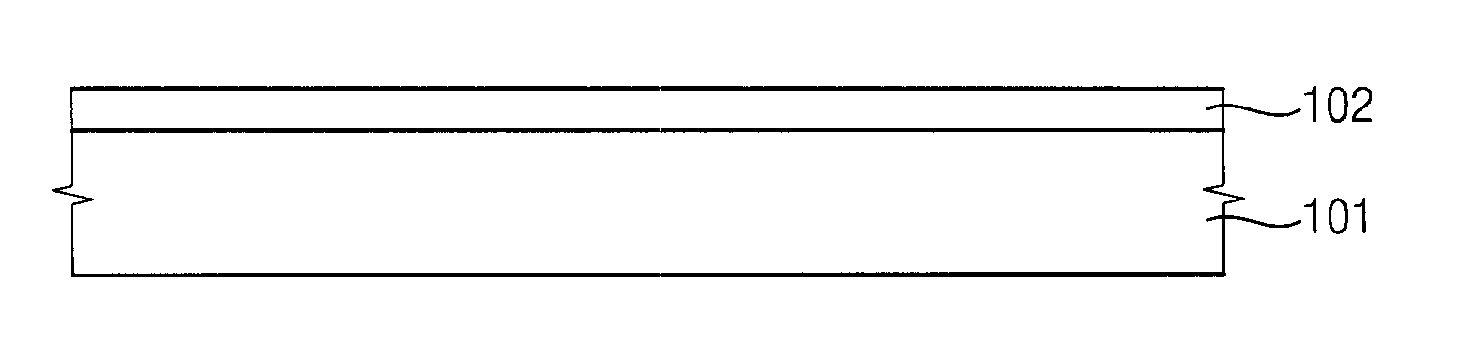
[0047]A base layer 102 is formed on the substrate 101. The base layer 102 may be an insulating layer, such as a silicon oxide layer, a silicon nitride layer, a silicon oxynitride layer, or stacked layers thereof. The base layer 102 may be formed by a sputtering method or a CVD method. Note that the base layer 102 may be omitted.
[0048]Referring to FIG. 3B, an oxide semiconductor layer 103 ma...
PUM
| Property | Measurement | Unit |
|---|---|---|
| temperature | aaaaa | aaaaa |
| thickness | aaaaa | aaaaa |
| pressure | aaaaa | aaaaa |
Abstract
Description
Claims
Application Information