

LED package
a technology of led packaging and led light, applied in the direction of basic electric elements, electrical equipment, semiconductor devices, etc., can solve the problems of overcoming certain light illumination uniformity challenges and bad effects on the use of led
- Summary
- Abstract
- Description
- Claims
- Application Information
AI Technical Summary
Problems solved by technology
Method used
Image

Examples
first embodiment
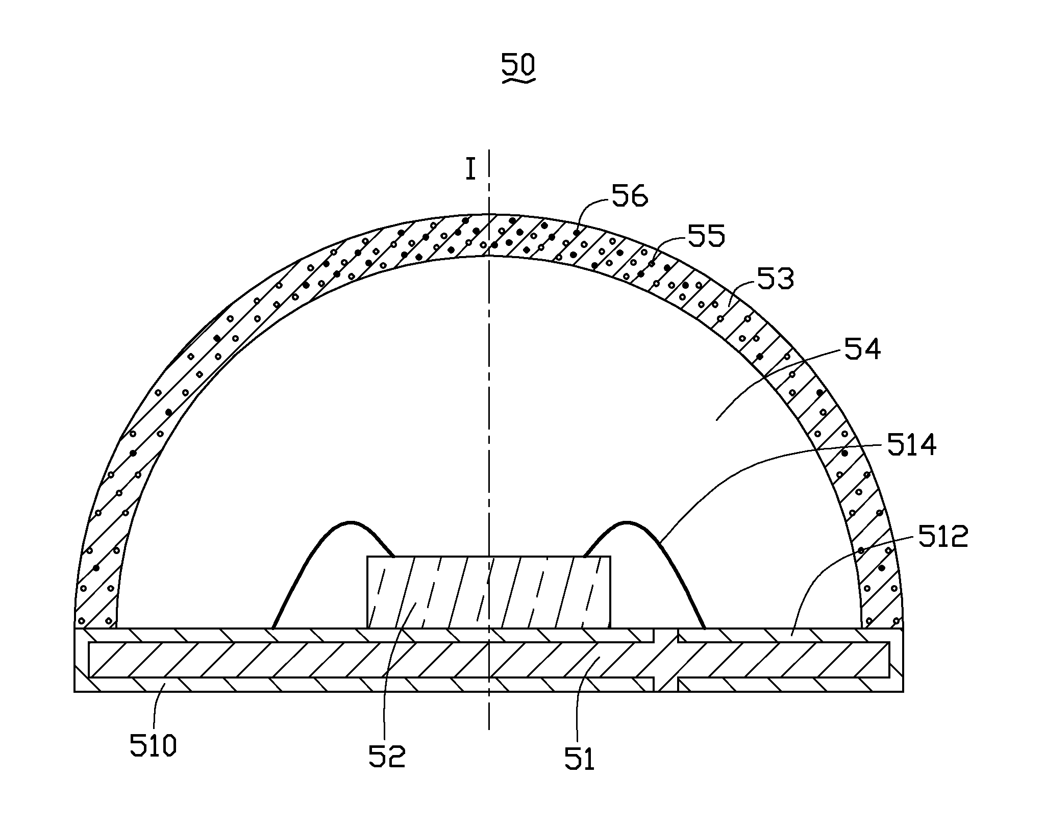
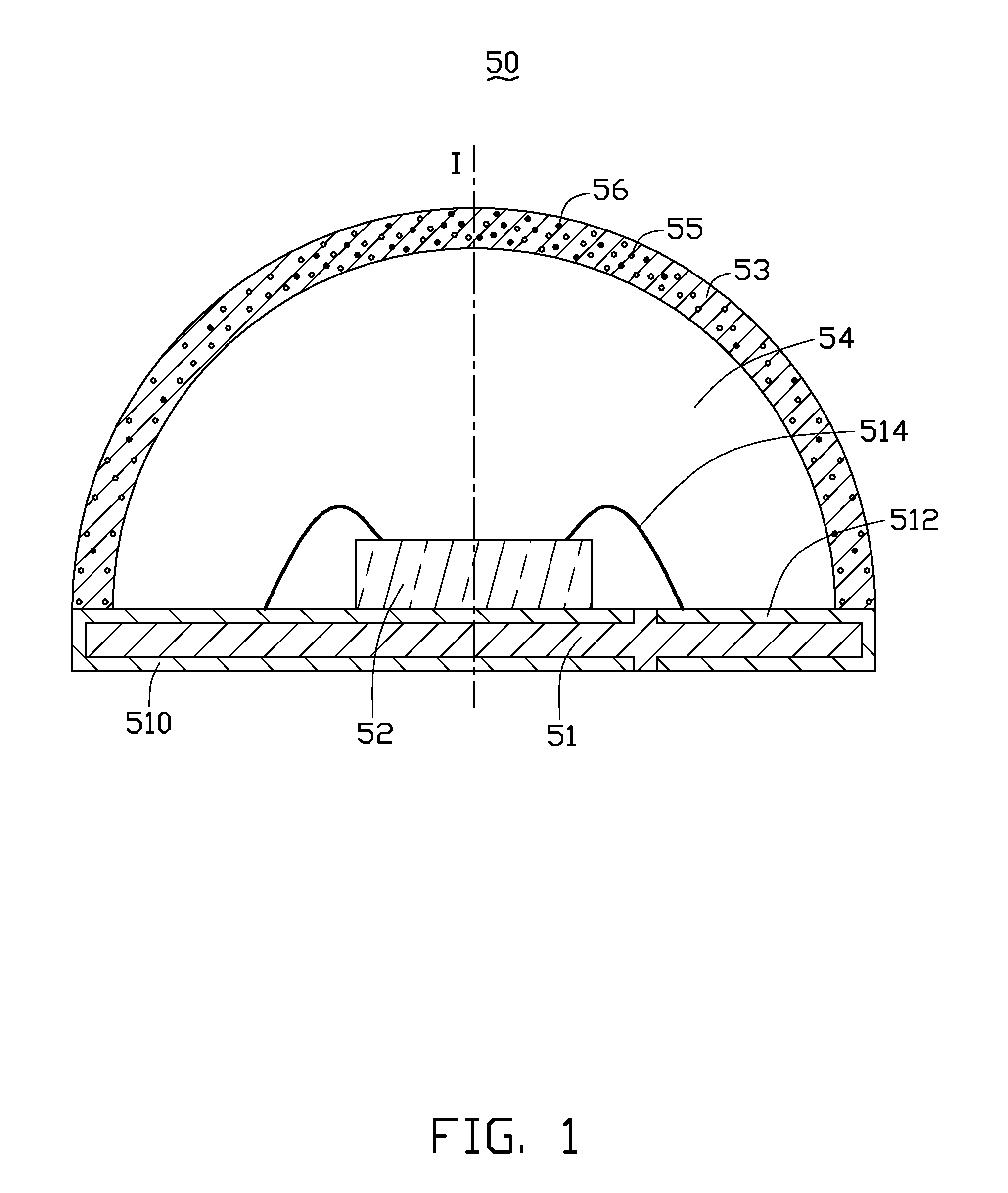
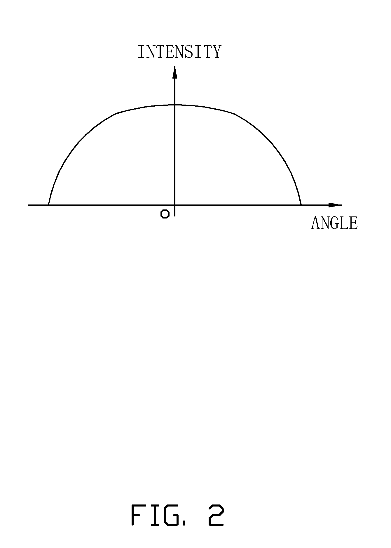
[0020]Referring to FIG. 1, an LED package 50 in accordance with a first embodiment includes a substrate 51, an LED die 52 arranged on the substrate 51, an encapsulating layer 53 covering the LED die 52, and a light dispersing element inside the encapsulating layer 53. The encapsulating layer 53 includes a luminescent material 55. The density of the light dispersing element is proportional to the intensity of light illuminated on the encapsulating layer 53.
[0021]The substrate 51 is Al2O3, silicon, SiC, ceramic, polymer, or insulant quartz. The substrate 51 includes a circuit electrically connecting with the LED die 52. The circuit includes a first electrode 510 and a second electrode 512. The LED die 52 is arranged on the first electrode 510 and electrically connecting with the first electrode 510 and the second electrode 512 through wires 514. The LED die 52 can also be arranged by manner of flip-chip (not shown). The first electrode 510 and the second electrode 512 of the circuit e...
second embodiment
[0028]Referring to FIG. 4, an LED package in accordance with a second embodiment includes an encapsulating layer 53b directly covering the LED die 52b by molding. The luminescent material 55b and the light scattering particles 56b are arranged inside the encapsulating layer 53b.
[0029]Referring to FIG. 5, an LED package 40 in accordance with a third embodiment includes a substrate 41, an LED die 42 arranged on the substrate 41, an encapsulating layer 43 covering the LED die 42, and a luminescent material 45 inside the encapsulating layer 43. The difference from the first embodiment is that there is no light scattering particles in the encapsulating layer 43 and the outer surface of the encapsulating layer 43 includes an atomization layer 46 as light dispersing element by atomization treatment. The degree of atomization is proportional to the light intensity illuminated on the encapsulating layer 43 from the LED die 42. In this embodiment, the degree of atomization is higher at the c...
PUM
 Abstract
Description
Claims
Application Information