

Electronic component
- Summary
- Abstract
- Description
- Claims
- Application Information
AI Technical Summary
Benefits of technology
Problems solved by technology
Method used
Image

Examples
Embodiment Construction
[0015]Hereinafter, an electronic component according to a preferred embodiment of the present invention will be described with reference to the drawings.
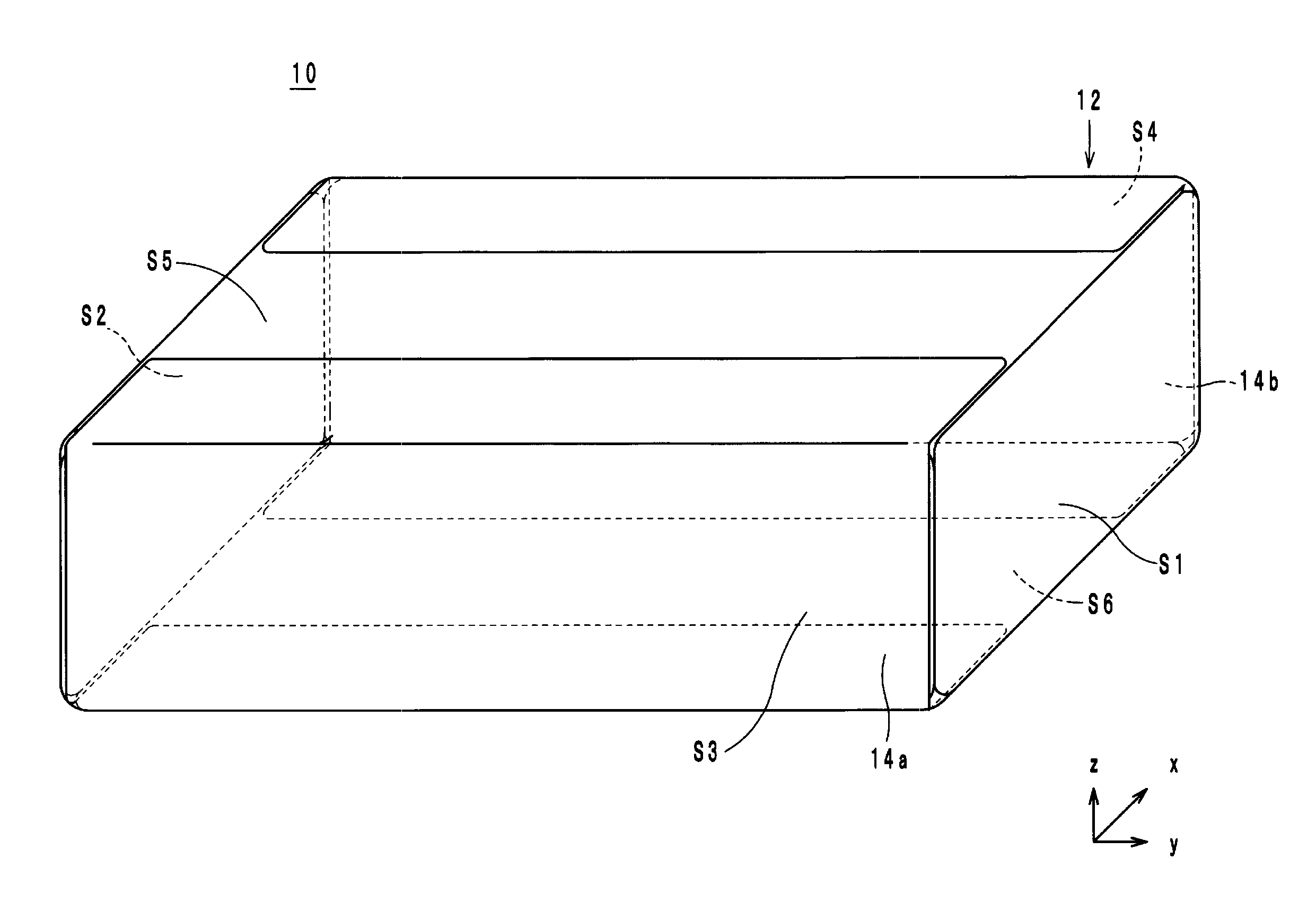
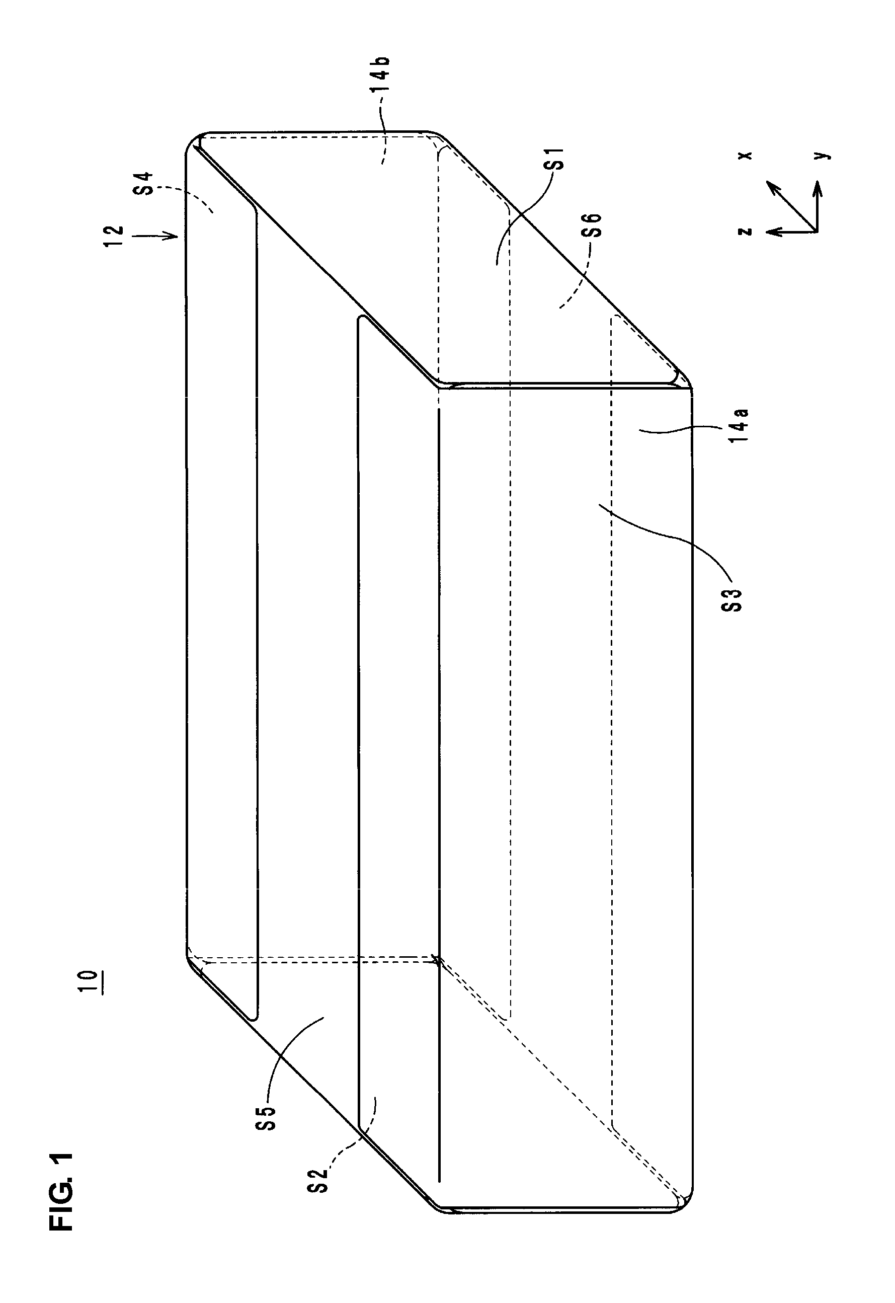
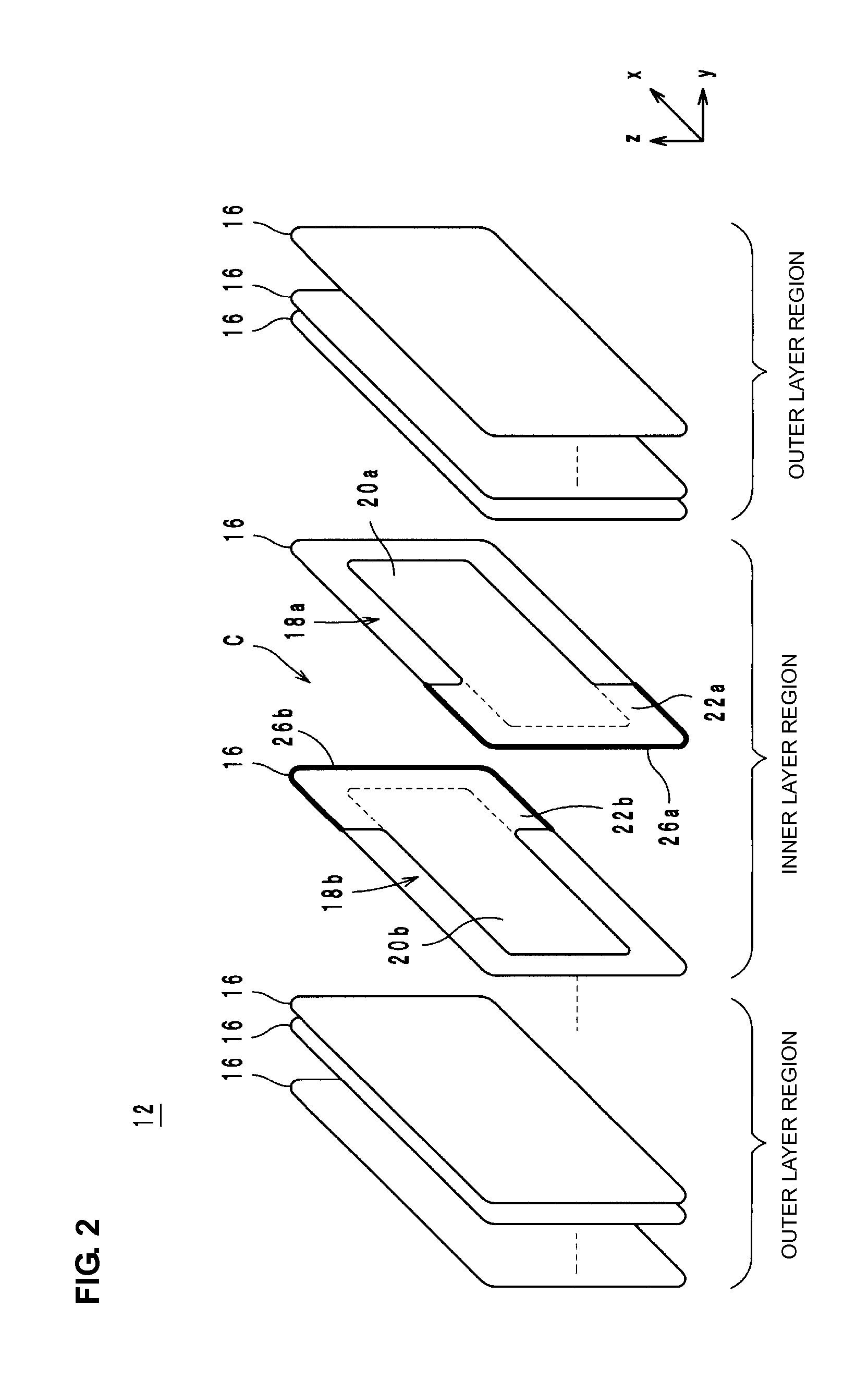
[0016]The structure of the electronic component will be described with reference to the drawings. FIG. 1 is a perspective view of an electronic component 10. FIG. 2 is an exploded perspective view of a laminate 12 of the electronic component 10. Hereinafter, the lamination direction of the laminate 12 is defined as a y axis direction. When the laminate 12 is viewed in plan in the y axis direction, a shorter side direction of the laminate 12 is defined as a z axis direction. When the laminate 12 is viewed in plan in the y axis direction, a longer side direction of the laminate 12 is defined as an x axis direction.
[0017]As shown in FIGS. 1 and 2, the electronic component 10 is a chip capacitor which includes the laminate 12, external electrodes 14 (14a and 14b), and a capacitor C (not shown in FIG. 1). The laminate 12 preferably has a...
PUM
 Abstract
Description
Claims
Application Information