

Optical device and analyzing apparatus
Inactive Publication Date: 2011-11-17
SEIKO EPSON CORP
View PDF3 Cites 7 Cited by
- Summary
- Abstract
- Description
- Claims
- Application Information
AI Technical Summary
Benefits of technology
[0008]An advantage of some aspects of the invention is to provide an optical device in
Problems solved by technology
Thus, only apart of the light concentrated by an objective lens is coupled to the surface plasmo
Method used
View moreImage
Smart ImageViewing Examples

Examples
 PUM
 Abstract
An optical device includes a projection group in which electrically conductive projections are arranged along a direction parallel to a virtual plane. The arrangement period of the projections in the projection group includes at least a first period and a second period different from the first period. The first period and the second period are shorter than a wavelength of an incident light.
Description
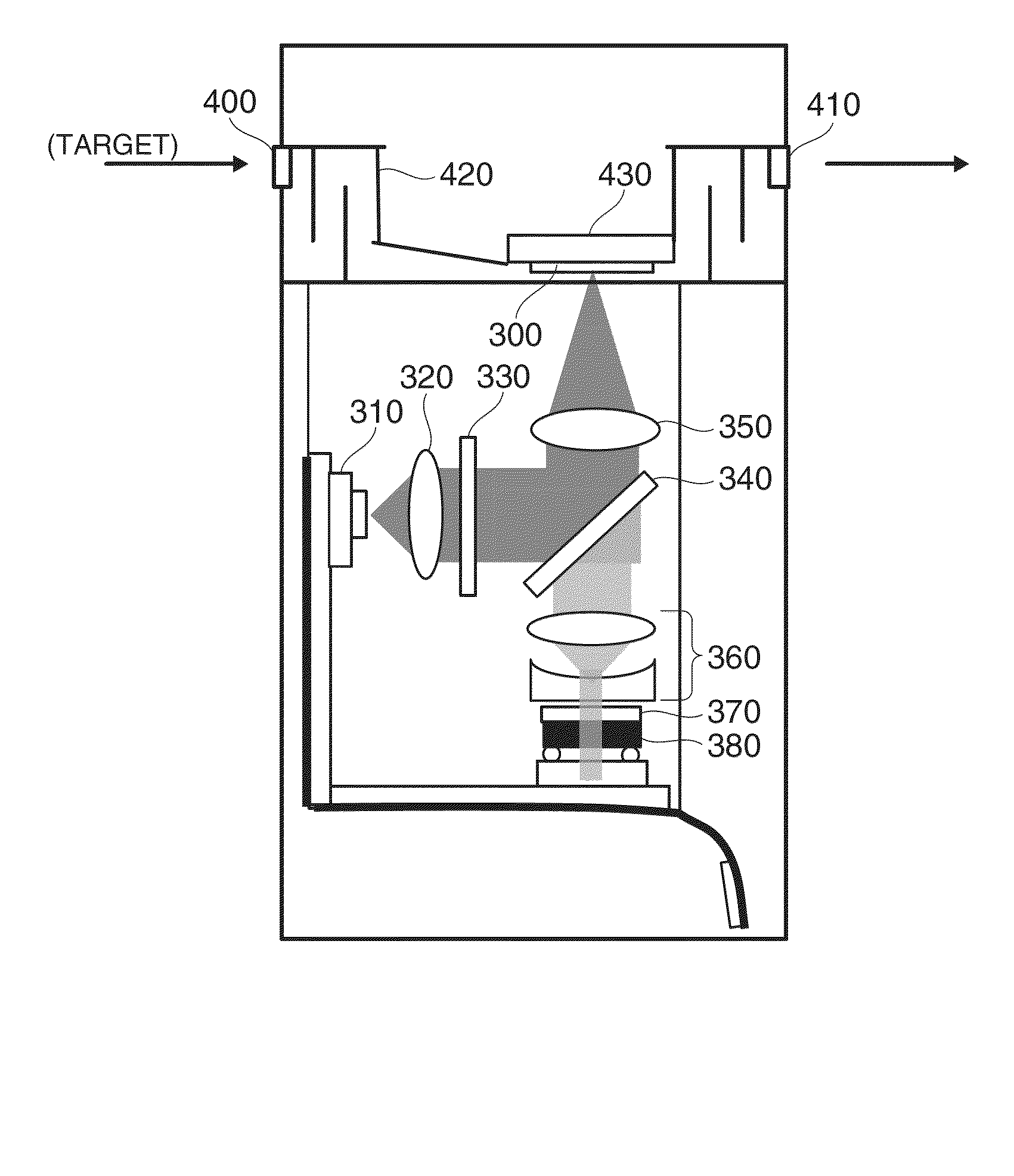
[0001]This application claims priority to Japanese Patent Application No. 2010-111144 filed May 13, 2010 which is hereby expressly incorporated by reference herein in its entirety.BACKGROUND[0002]1. Technical Field[0003]The present invention relates to an optical device and an analyzing apparatus.[0004]2. Related Art[0005]In recent years, the demand for a sensor used for medical diagnosis, food inspection or the like has increased, and the development of a highly sensitive small sensor has been requested. In order to meet such request, various types of sensors including one using an electrochemical technique have been studied. Among these, interest in a sensor using surface plasmon resonance has increased because the sensor can be integrated, manufactured at low cost, and used in any measurement environment.[0006]For example, JP-A-2007-240361 discloses a surface plasmon resonance sensor in which light is coupled to a surface plasmon polariton by a metal periodic structure.[0007]Howe...
Claims
Login to View More Application Information
Patent Timeline
 IPC IPC(8): G01J3/44G01N21/55G01N21/65
CPCG01N21/658G01N21/554G01N21/27G01N21/65A61B5/00
InventorAMAKO, JUNYAMADA, KOHEI
OwnerSEIKO EPSON CORP