Optical reflection element

a reflection element and optical technology, applied in the field of optical reflection elements, can solve the problems of reducing the detection accuracy of the monitor element, unable to perform unable to achieve self-excited driving of the optical reflection element, so as to achieve high detection accuracy, high detection accuracy, and high detection accuracy

Active Publication Date: 2011-12-01
PANASONIC CORP
View PDF4 Cites 55 Cited by
  • Summary
  • Abstract
  • Description
  • Claims
  • Application Information

AI Technical Summary

Benefits of technology

[0013]An object of the present invention is to provide an optical reflection element having a monitor element with high detection accuracy, thereby performing self-excited driving with high accuracy.
[0014]The optical reflection element of the present invention includes a mirror portion, and an oscillator coupled to the mirror portion. The oscillator includes a base, an insulating layer, a drive element, and a monitor element. The insulating layer is formed on the base. The drive element and the monitor element are formed on the insulating layer, and are separated from each other by a separation groove. Each of the drive element and the monitor element includes a lower electrode layer, a piezoelectric layer, and an upper electrode layer formed in that order on the insulating layer. The lower electrode layer of the drive element and the lower electrode layer of the monitor element are connected to the same external electrode. The separation groove allows the shortest conductive path between an arbitrary point of the lower electrode layer of the monitor element and an arbitrary point of the lower electrode layer of the drive element adjacent to the monitor element to be set to be longer than the distance from the arbitrary point of the lower electrode layer of the monitor element to the external electrode.
[0015]The optical reflection element of the present invention has a monitor element with high detection accuracy, thereby performing self-excited driving with high accuracy.
[0016]More specifically, the ground resistance of the lower electrode of the monitor element can be made lower than the conductive resistance between the lower electrode of the monitor element and the lower electrode of the drive element.
[0017]This structure can prevent current leakage between the upper electrode layer of the monitor element and the upper electrode layer of the drive element even when the lower electrode layer is arranged lengthwise.
[0018]As a result, the monitor element has high detection accuracy, allowing the optical reflection element to perform self-excited driving with high accuracy.

Problems solved by technology

In this example, however, when the driving frequency is too high, the optical reflection element sometimes cannot perform self-excited driving.
This decreases the detection accuracy of the monitor element, making is impossible for the optical reflection element to perform self-excited driving.

Method used


Image

  • Optical reflection element
  • Optical reflection element
  • Optical reflection element

Examples


first exemplary embodiment

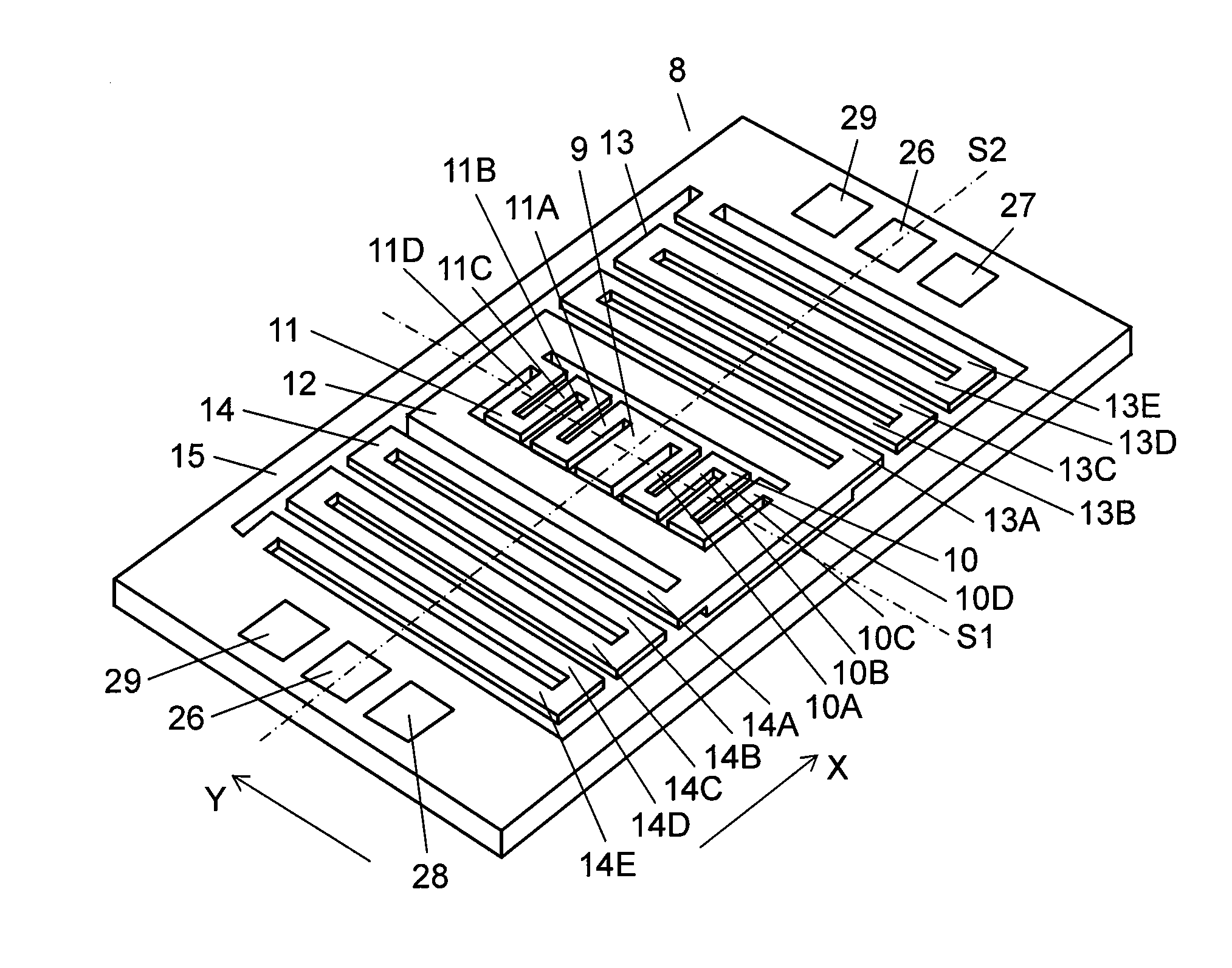
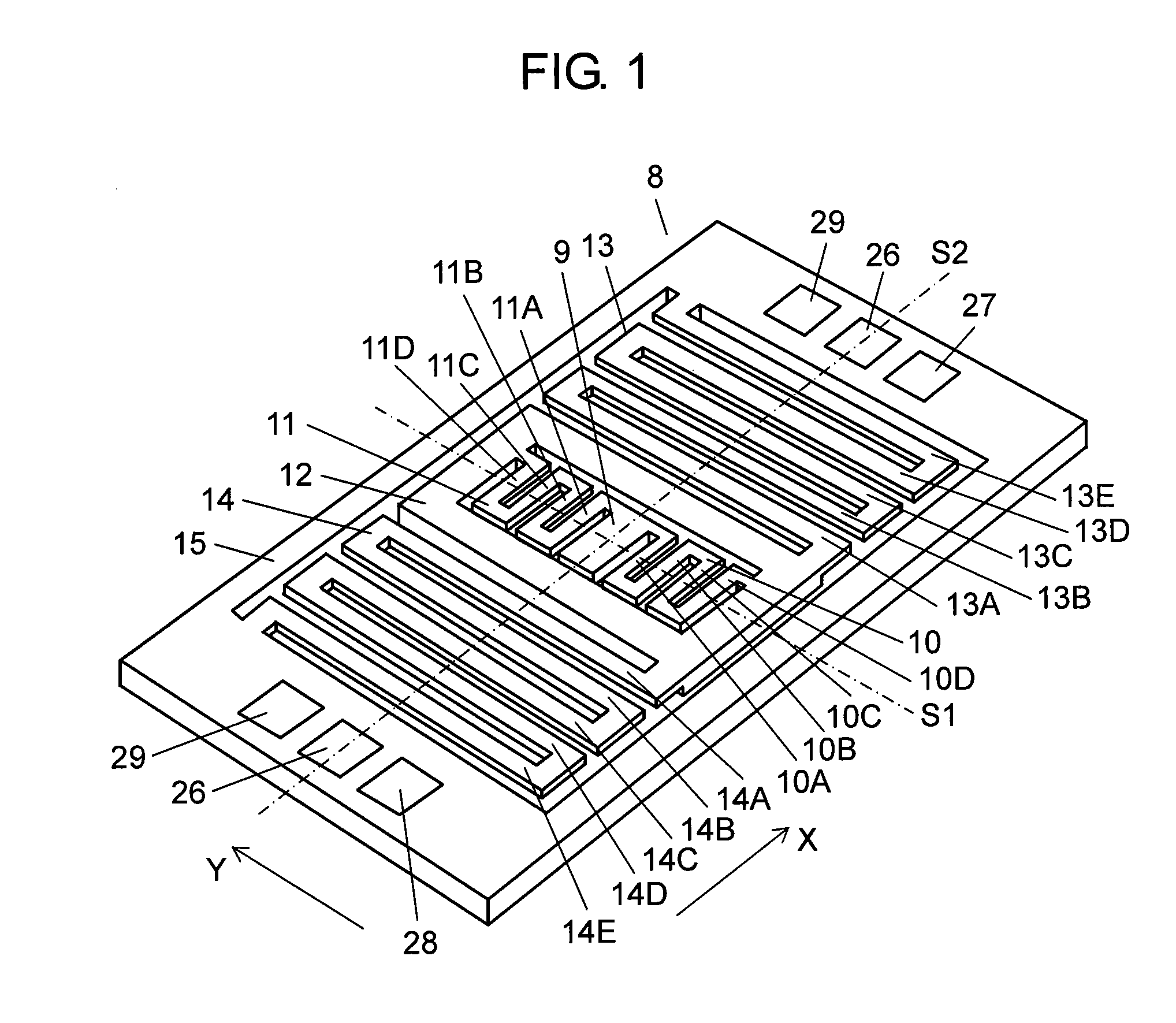
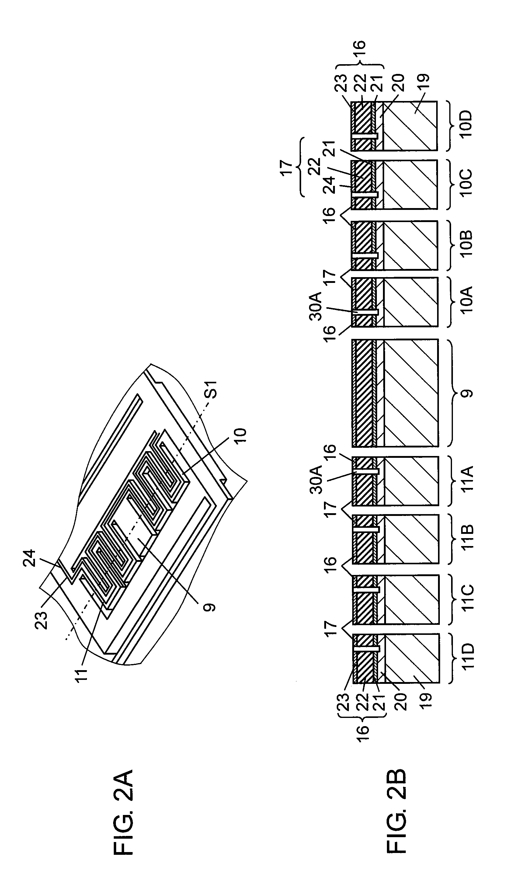
[0030]The structure of an optical reflection element of the present exemplary embodiment will be described as follows with reference to FIGS. 1 to 4. FIG. 1 is a perspective view of the optical reflection element. FIGS. 2A and 2B are a perspective view and a sectional view, respectively, of first oscillators in the optical reflection element. FIGS. 3 and 4 are sectional views of one second oscillator and the other second oscillator, respectively, in the optical reflection element.

[0031]In FIG. 1, optical reflection element 8 of the present exemplary embodiment includes mirror portion 9 and a pair of first oscillators 10 and 11. First oscillators 10 and 11 are opposed to each other in the y-axis direction with mirror portion 9 therebetween, and are coupled to the ends of mirror portion 9. Optical reflection element 8 further includes frame body 12. Frame body 12 is coupled to first oscillators 10 and 11, and surrounds the outer peripheries of first oscillators 10, 11 and mirror porti...


PUM


Abstract

An optical reflection element includes a mirror portion and an oscillator coupled to the mirror portion. The oscillator includes a base, an insulating layer, a drive element, and a monitor element. The insulating layer is formed on the base. The drive element and the monitor element are formed on the insulating layer, and are separated from each other by a separation groove. Each of the drive element and the monitor element includes a lower electrode layer, a piezoelectric layer, and an upper electrode layer formed in that order on the insulating layer. The monitor element has high detection accuracy, allowing the optical reflection element to perform self-excited driving with high accuracy.

Description

[0001]This application is a U.S. National Phase Application of PCT international application PCT / JP2009 / 006190.TECHNICAL FIELD[0002]The present invention relates to an optical reflection element used in display and other devices.BACKGROUND ART[0003]FIG. 10 shows conventional optical reflection element 1. Optical reflection element 1 includes mirror portion 2, a pair of first oscillators 3 and 4, frame body 5, and a pair of second oscillators 6 and 7. First oscillators 3 and 4 are coupled to the ends of mirror portion 2. Frame body 5 is coupled to first oscillators 3 and 4, and surrounds the outer peripheries of first oscillators 3, 4 and mirror portion 2. Second oscillators 6 and 7 are coupled to the ends of frame body 5.[0004]First oscillators 3 and 4 have an axis S1 as their central axis, which is parallel to the y-axis. Second oscillators 6 and 7 have an axis S as their central axis, which is parallel to the x-axis. Thus, first oscillators 3, 4 and second oscillators 6, 7 are for...

Claims


Application Information

Patent Timeline
Patent Type & Authority Applications(United States)
IPC IPC(8): G02B26/08
CPCG02B26/101G02B26/0858G02B5/08G02B26/08
Inventor HIRAOKA, SOICHIROTERADA, JIROUNAKAZONO, SHINSUKEFURUKAWA, SHIGEOFURUKAWA, KIYOMI
Owner PANASONIC CORP
Why Eureka
Try Eureka