Manufacturing method of gate stack and semiconductor device

a manufacturing method and gate stack technology, applied in the field of semiconductor technology, can solve the problems of difficult to achieve eot1 nm, small eot is difficult to achieve, and the layer might not be fully formed, and achieve the effect of unstable work function

Active Publication Date: 2011-12-08
INST OF MICROELECTRONICS CHINESE ACAD OF SCI
View PDF32 Cites 42 Cited by
  • Summary
  • Abstract
  • Description
  • Claims
  • Application Information

AI Technical Summary

Benefits of technology

[0032]According to the present invention, after the selective etching process, the sacrificial oxygen-scavenging metal spacers are formed in the outer periphery of the gate stack structure (the interfacial oxide layer, the high-K dielectric layer, and the metal gate electrode) and are arranged along the sidewall of the gate stack structure, acting as a sacrificial layer of the oxygen-scavenging process. In this way, disadvantages such as the EOT increasing and work function instability possibly caused by the conventional process can be overcome. Further, optionally, the sacrificial oxygen-scavenging metal spacers can be disposed between the gate stack structure and the dielectric spacers and has a simple D-shape or an L-shape section.

Problems solved by technology

An interfacial layer between the high-K dielectric and the substrate channel (usually a semiconductor substrate) makes it very difficult to achieve EOT<1 nm, because the interfacial layer itself could account for about 4 Å thickness.
1. The sacrificial metal layer (the sacrificial oxygen-scavenging metal layer 140) becomes a metal oxide layer (dielectric layer) after the oxygen within the dielectric layer (the high-K dielectric layer 130) is scavenged by the sacrificial metal layer. This converted dielectric layer will be accounted for the new EOT increase and thereby small EOT is hard to achieve.
2. The sacrificial metal layer might not be fully converted into metal oxide dielectric (dielectric layer) if, for example, oxygen is not enough for the complete conversion of the sacrificial metal layer. This could result in thickness variation for the metal oxide (dielectric layer), and thereby variation of work functions for different devices.

Method used


Image

  • Manufacturing method of gate stack and semiconductor device
  • Manufacturing method of gate stack and semiconductor device
  • Manufacturing method of gate stack and semiconductor device

Examples


first embodiment

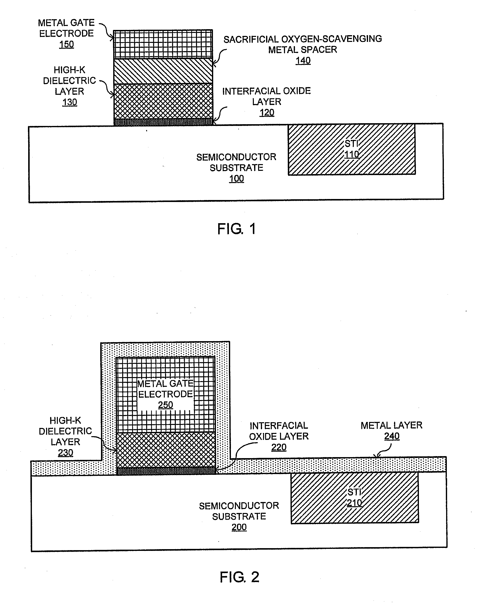
[0041]The semiconductor device manufactured by the gate stack manufacturing method according to the first embodiment of the present application is described with reference to FIG. 5. FIG. 5 is a schematic view of the semiconductor device obtained by the gate stack manufacturing method according to the first embodiment of the present invention.

[0042]As shown in FIG. 5, the semiconductor device obtained by the gate stack manufacturing method according to the first embodiment of the present invention mainly comprises: a semiconductor substrate 200, an STI (Shallow Trench Isolation) 210, an interfacial oxide layer 220, a high-K dielectric layer 230, a metal gate electrode 250, sacrificial oxygen-scavenging metal spacers 240, and dielectric spacers 260 (optional). The STI 210 is formed in the semiconductor substrate 200 for isolating the gate and the source / drain. The interfacial oxide layer 220 is formed on the semiconductor substrate 200. The high-K dielectric layer 230 is formed on th...

second embodiment

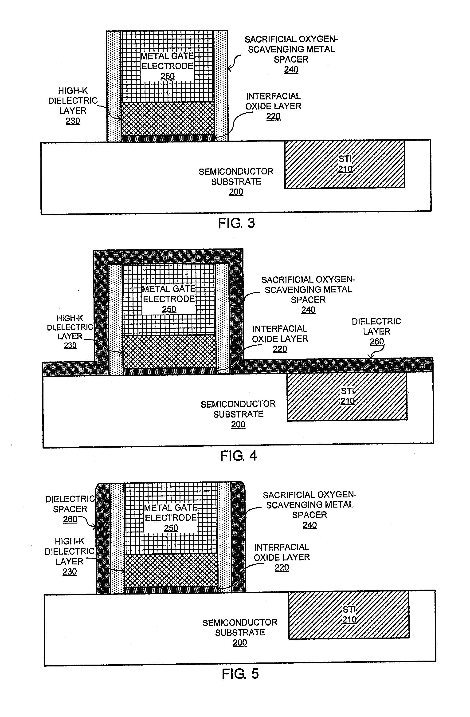
[0053]The semiconductor device manufactured by the gate stack manufacturing method according to the second embodiment of the present application is described with reference to FIG. 7. FIG. 7 is a schematic view of the semiconductor device obtained by the gate stack manufacturing method according to the second embodiment of the present invention.

[0054]As shown in FIG. 7, the semiconductor device obtained by the gate stack manufacturing method according to the second embodiment of the present invention mainly comprises: a semiconductor substrate 200, an STI (shallow trench isolation) 210, an interfacial oxide layer 220, a high-K dielectric layer 230, a metal gate electrode 250, sacrificial oxygen-scavenging metal spacers 240, and dielectric spacers 260. The STI 210 is formed in the semiconductor substrate 200 for isolation of devices. The interfacial oxide layer 220 is formed on the semiconductor substrate 200. The high-K dielectric layer 230 is formed on the interfacial oxide layer 2...

third embodiment

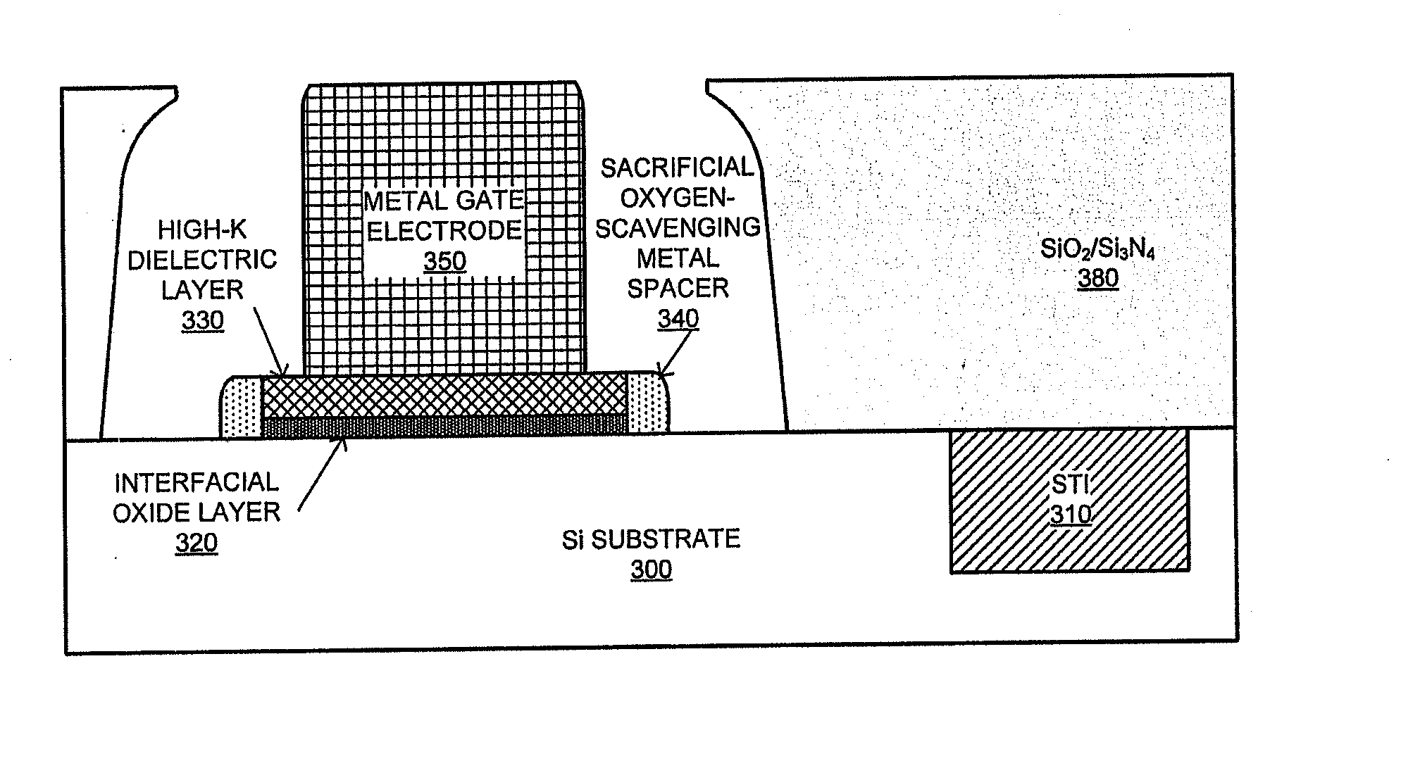
[0063]The semiconductor device manufactured by the gate stack manufacturing method according to the third embodiment of the present application is described with reference to FIGS. 11 and 12. FIGS. 11 and 12 are schematic views of the semiconductor devices obtained by the gate stack manufacturing method according to the third embodiment of the present invention.

[0064]As shown in FIG. 11, the semiconductor device obtained by the gate stack manufacturing method according to the third embodiment of the present invention mainly comprises: a semiconductor substrate 300, an STI (shallow trench isolation) 310, an interfacial oxide layer 320, a high-K dielectric layer 330, a metal gate electrode 350, sacrificial oxygen-scavenging metal spacers 340, dielectric spacers 360, spacers 370, and an inter-device isolation dielectric layer (SiO2 / Si3N4) 380. The STI 310 is formed in the semiconductor substrate 300 for isolating the gate and the source / drain. The interfacial oxide layer 320, the high-...


PUM

PropertyMeasurementUnit
heightaaaaaaaaaa
widthaaaaaaaaaa
widthaaaaaaaaaa

Abstract

A manufacturing method of a gate stack with sacrificial oxygen-scavenging metal spacers includes: forming a gate stack structure consisting of an interfacial oxide layer, a high-K dielectric layer and a metal gate electrode, on a semiconductor substrate; conformally depositing a metal layer covering the semiconductor substrate and the gate stack structure; and selectively etching the metal layer to remove the portions of the metal layer covering the top surface of the gate stack structure and the semiconductor substrate, so as to only keep the sacrificial oxygen-scavenging metal spacers surrounding the gate stack structure in the outer periphery of the gate stack structure. A semiconductor device manufactured by this process.

Description

BACKGROUND OF THE INVENTION[0001]1. Field of the Invention[0002]The invention relates to the technology of semiconductor, and particularly to a semiconductor device and a manufacturing method of the same. More particularly, it relates to a manufacturing method of a gate stack with sacrificial oxygen-scavenging metal spacers, and a semiconductor device with a gate stack structure manufactured by the method.[0003]2. Description of the Prior Art[0004]Conventional Complementary Metal Oxide Semiconductor Field Effect Transistor (CMOSFET) manufacturing process comprises Gate-First process and Gate-Last process. High-dielectric-constant(high-K) dielectric / metal gate electrode stacks with Low equivalent oxide thickness (EOT) are widely used in 32 nm technology node and beyond. An interfacial layer between the high-K dielectric and the substrate channel (usually a semiconductor substrate) makes it very difficult to achieve EOT<1 nm, because the interfacial layer itself could account for a...

Claims


Application Information

Patent Timeline
Patent Type & Authority Applications(United States)
IPC IPC(8): H01L29/78H01L21/3205B82Y40/00B82Y99/00
CPCH01L21/28176H01L29/513H01L29/517H01L29/78H01L29/66545H01L29/66553H01L29/6656H01L29/6653
Inventor ZHONG, HUICAILUO, ZHIJIONGLIANG, QINGQING
Owner INST OF MICROELECTRONICS CHINESE ACAD OF SCI
Why Eureka
Try Eureka