Semiconductor package and method of manufacturing the semiconductor package

a semiconductor and semiconductor technology, applied in the direction of semiconductor devices, semiconductor/solid-state device details, electrical apparatus, etc., can solve the problems of affecting the efficiency of signal transfer, not only disturbing other semiconductor chips, and harming the human body

Inactive Publication Date: 2011-12-08
SAMSUNG ELECTRO MECHANICS CO LTD
View PDF3 Cites 5 Cited by
  • Summary
  • Abstract
  • Description
  • Claims
  • Application Information

AI Technical Summary

Benefits of technology

[0008]The present invention provides a semiconductor package and a method of manufacturing the semiconductor package that can block electromagnetic waves between semiconductor chips mounted inside the semiconductor package.

Problems solved by technology

The electromagnetic waves not only disturb other semiconductor chips or lower the efficiency of signal transfer but also are harmful to the human body.
However, although the shielding technology was able to block the electromagnetic waves emitted to the outside of the semiconductor package or the electromagnetic waves permeated into the semiconductor package from the outside, it has not been able to block the electromagnetic waves between the semiconductor chips within the semiconductor package.
Moreover, the shielding member and a ground circuit need to be connected to each other, but it has been difficult to provide a connection space between the shielding member and the ground circuit as the semiconductor package becomes smaller and thinner.

Method used


Image

  • Semiconductor package and method of manufacturing the semiconductor package
  • Semiconductor package and method of manufacturing the semiconductor package
  • Semiconductor package and method of manufacturing the semiconductor package

Examples


Embodiment Construction

[0024]Hereinafter, some embodiments of the present invention will be described with reference to the accompanying drawings.

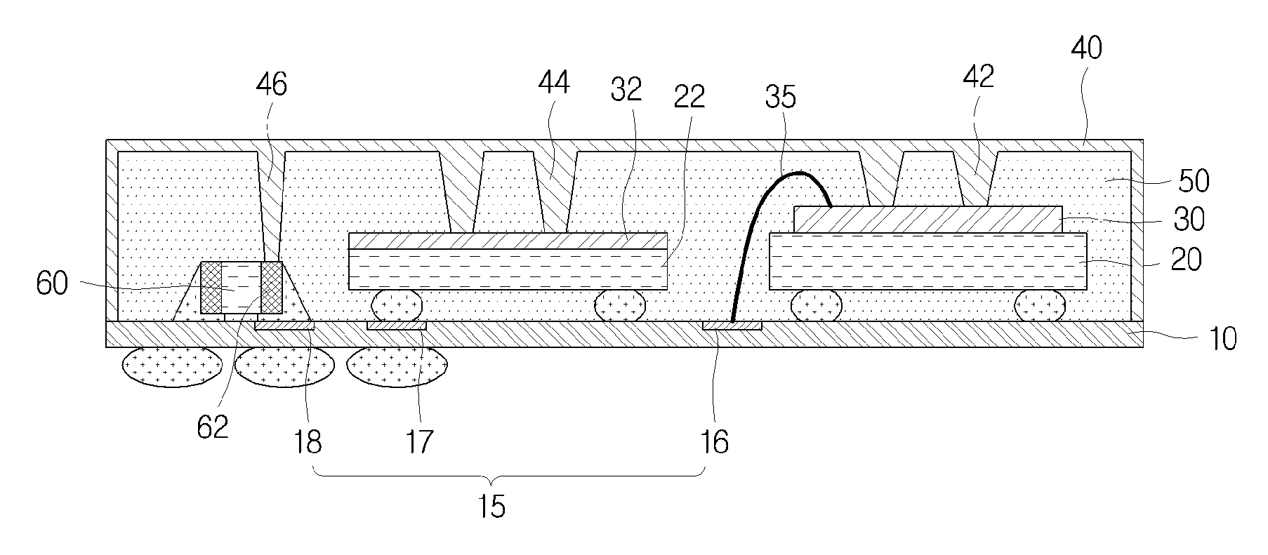
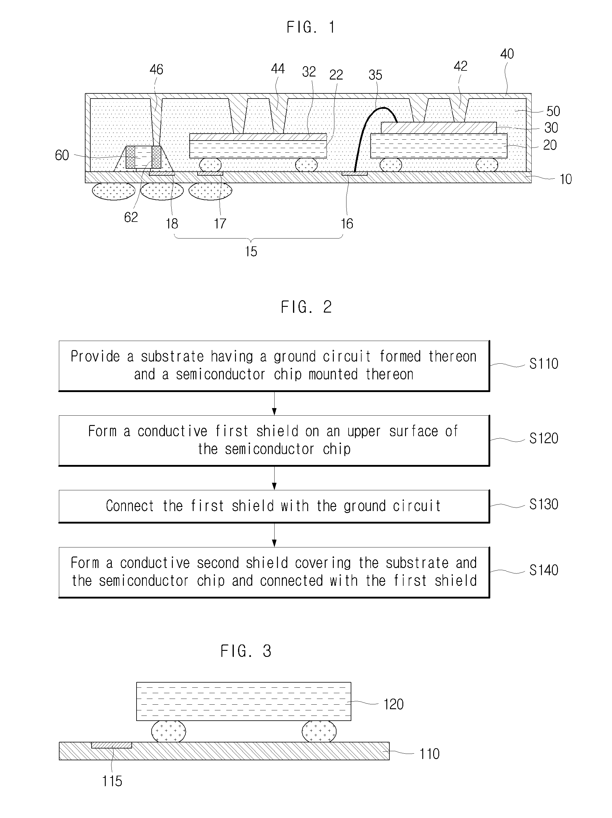
[0025]FIG. 1 is a sectional view of a semiconductor package in accordance with an embodiment of the present invention.

[0026]The semiconductor package in accordance with an embodiment of the present invention includes a substrate 10, a semiconductor chip 20, a first shield 30 and a second shield 40.

[0027]The substrate 10 is where the semiconductor chip 20 is mounted, and is formed with a circuit pattern, which is connected to the semiconductor chip 20, and a ground circuit 15, which is needed for shielding.

[0028]In the present embodiment, the semiconductor chip 20 is mounted on one surface of the substrate 10, and the ground circuit 15 includes ground pads 16, 17, 18 required for grounding.

[0029]The semiconductor chip 20 is an electronic part in which a variety of devices are integrated to perform certain functions and is mounted on one surface of the substrate 1...


PUM


Abstract

A semiconductor package and a method of manufacturing the semiconductor package are disclosed. A semiconductor package in accordance with an embodiment of the present invention includes a substrate, which has a ground circuit formed thereon, a semiconductor chip, which is mounted on the substrate, a conductive first shield, which is formed on an upper surface of the semiconductor chip and connected with the ground circuit, and a conductive second shield, which covers the substrate and the semiconductor chip and is connected with the first shield. With a semiconductor package in accordance with an embodiment of the present invention, grounding is possible between semiconductor chips because a shield is also formed on an upper surface of the semiconductor chip, and the shielding property can be improved by a double shielding structure.

Description

CROSS-REFERENCE TO RELATED APPLICATIONS[0001]This application claims the benefit of Korean Patent Application No. 10-2010-0052413, filed with the Korean Intellectual Property Office on Jun. 3, 2010, the disclosure of which is incorporated herein by reference in its entirety.BACKGROUND[0002]1. Technical Field[0003]The present invention is related to a semiconductor package and a method of manufacturing the semiconductor package.[0004]2. Description of the Related Art[0005]It is common that electromagnetic waves are generated from a semiconductor chip mounted in a semiconductor package. The electromagnetic waves not only disturb other semiconductor chips or lower the efficiency of signal transfer but also are harmful to the human body.[0006]Developed accordingly is a shielding technology that covers the semiconductor package with a conductive shielding member. However, although the shielding technology was able to block the electromagnetic waves emitted to the outside of the semicondu...

Claims


Application Information

Patent Timeline
Patent Type & Authority Applications(United States)
IPC IPC(8): H01L23/552H01L21/02
CPCH01L23/3121H01L23/552H01L24/16H01L24/29H01L24/73H01L2224/16225H01L2924/1815H01L2224/73253H01L2924/19107H01L2924/01033H01L2924/19105H01L2924/15311H01L2224/291H01L2224/73209
Inventor YOO, DO-JAEDOH, JAE-CHEON
Owner SAMSUNG ELECTRO MECHANICS CO LTD
Why Eureka
Try Eureka