Focus Compensation For Optical Elements And Applications Thereof

a technology of optical elements and compensation, applied in the field of optical elements, can solve the problems of only magnifying inefficiencies, significantly increasing costs and time of manufacture, and effectively administering the focus adjustment of the optical element of each module serially, so as to avoid one or more inefficiencies and reduce the cost and time of production of optical imaging apparatus

Active Publication Date: 2011-12-15
FLIR SYSTEMS TRADING BELGIUM BVBA
View PDF1 Cites 22 Cited by
  • Summary
  • Abstract
  • Description
  • Claims
  • Application Information

AI Technical Summary

Benefits of technology

[0006]In view of the foregoing disadvantages, the present invention provides optical imaging apparatus having the desired focal properties, which can be manufactured and/or assembled at the wafer level. Wa

Problems solved by technology

A disadvantage of the foregoing manufacturing technique is that the focus adjustment for the optical element of each module is effectively administered serially.
Manufacturing solid state camera m

Method used


Image

  • Focus Compensation For Optical Elements And Applications Thereof
  • Focus Compensation For Optical Elements And Applications Thereof
  • Focus Compensation For Optical Elements And Applications Thereof

Examples


Embodiment Construction

[0036]The present invention can be understood more readily by reference to the following detailed description, examples and drawings and their previous and following descriptions. Elements, apparatus and methods of the present invention, however, are not limited to the specific embodiments presented in the detailed description, examples and drawings. It should be recognized that these embodiments are merely illustrative of the principles of the present invention. Numerous modifications and adaptations will be readily apparent to those of skill in the art without departing from the spirit and scope of the invention.

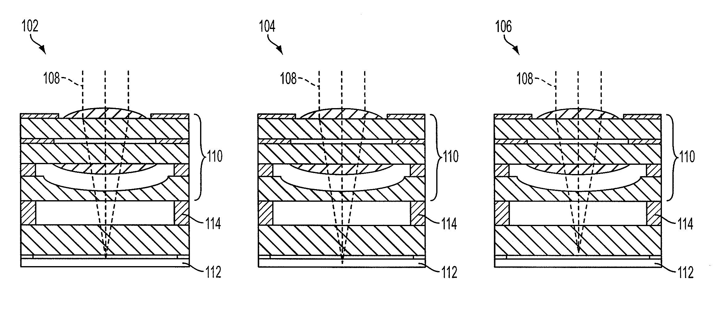
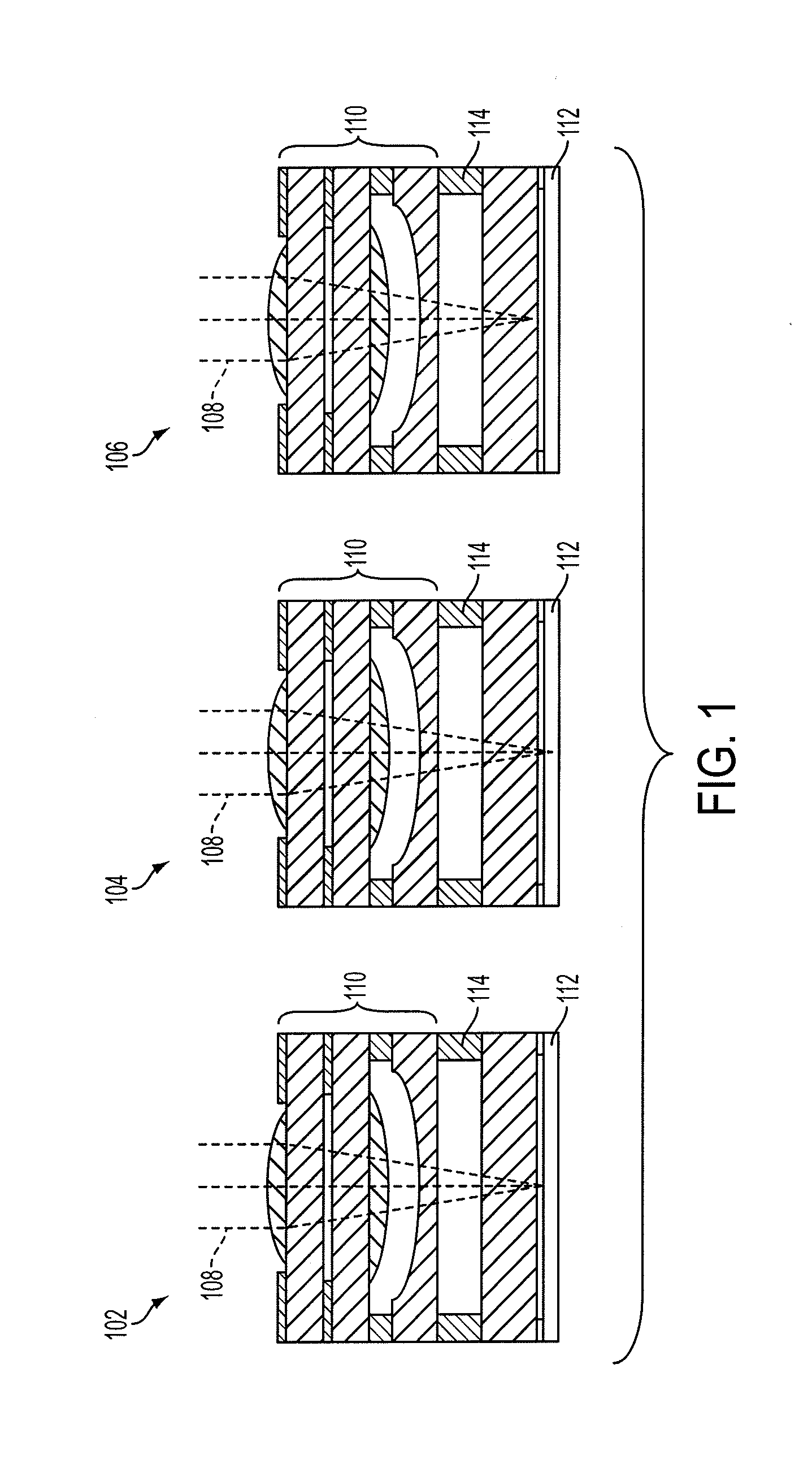
[0037]The present invention provides optical imaging apparatus having the desired focal properties, which can be manufactured and / or assembled at the wafer level. Wafer level assembly, in some embodiments, can offer cost and time efficient production of optical imaging apparatus while avoiding one or more inefficiencies associated with serial manufacturing and / or focusing ...


PUM


Abstract

Optical imaging apparatus are provided having the desired focal properties, which can be manufactured and/or assembled at the wafer level.

Description

RELATED APPLICATION DATA[0001]The present application claims priority pursuant to 35 U.S.C. §119(e) to U.S. Provisional Patent Application Ser. No. 61 / 253,337, filed Oct. 20, 2009 which is hereby incorporated by reference in its entirety.FIELD OF THE INVENTION[0002]The present invention relates to optical elements and, in particular, to optical elements used in optical imaging apparatus.BACKGROUND OF THE INVENTION[0003]Optical imaging apparatus incorporating solid state sensing elements find application in a variety of fields ranging from military reconnaissance and surveillance to consumer electronics. Solid state cameras, for example, are used in a number of consumer electronics including cell phones, digital still cameras, computers, toys and automotive driver aids. In order to satisfy demand, solid state cameras are required to be manufactured in significant quantities ordering on the millions per day. In view of these numbers, efficient and low cost manufacture of solid state c...

Claims


Application Information

Patent Timeline
IPC IPC(8): G02B11/02G02B7/02
CPCH01L27/14618H01L27/14625H04N5/2257H01L27/14685H01L27/14632H01L2924/0002H04N23/57H01L2924/00H01L27/14687
Inventor WELCH, WILLIAM HUDSONOVRUTSKY, DAVIDARANDA, ANDREW
Owner FLIR SYSTEMS TRADING BELGIUM BVBA
Why Eureka
Try Eureka