Image sensor and package including the image sensor

a technology of image sensor and package, applied in the direction of electrical equipment, semiconductor devices, radio frequency controlled devices, etc., can solve the problems of low power and relatively easy application of the technology to a product having a limited battery capacity

Active Publication Date: 2012-01-05
SAMSUNG ELECTRONICS CO LTD
View PDF4 Cites 85 Cited by
  • Summary
  • Abstract
  • Description
  • Claims
  • Application Information

AI Technical Summary

Problems solved by technology

In addition, since the CMOS image sensor consumes very low power, it may be relatively easy to apply it to a product having a limited battery capacity.

Method used


Image

  • Image sensor and package including the image sensor
  • Image sensor and package including the image sensor
  • Image sensor and package including the image sensor

Examples


Embodiment Construction

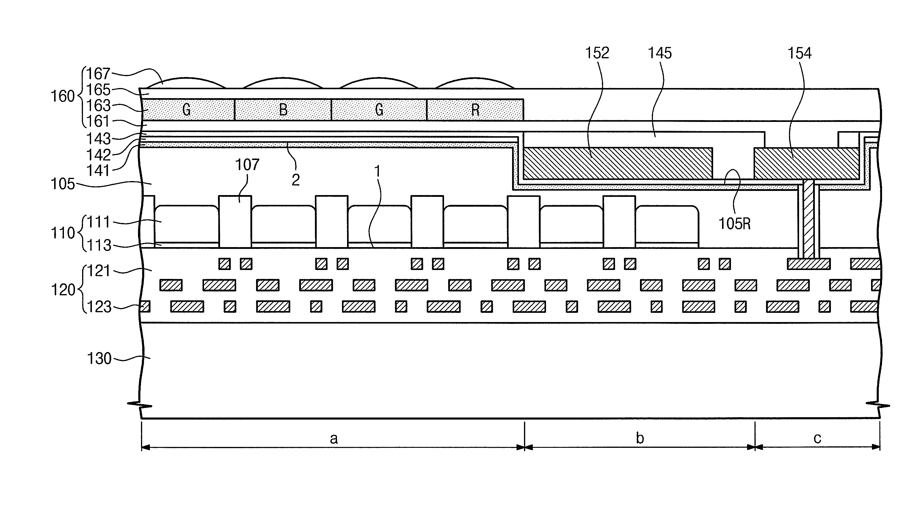
[0026]Preferred embodiments of the inventive concept will be described below in more detail with reference to the accompanying drawings. The embodiments of the inventive concept may, however, be embodied in different forms and should not be construed as limited to the embodiments set forth herein. Like numbers refer to like elements throughout.

[0027]The terminology used herein is for the purpose of describing particular embodiments only and is not intended to be limiting of the invention.

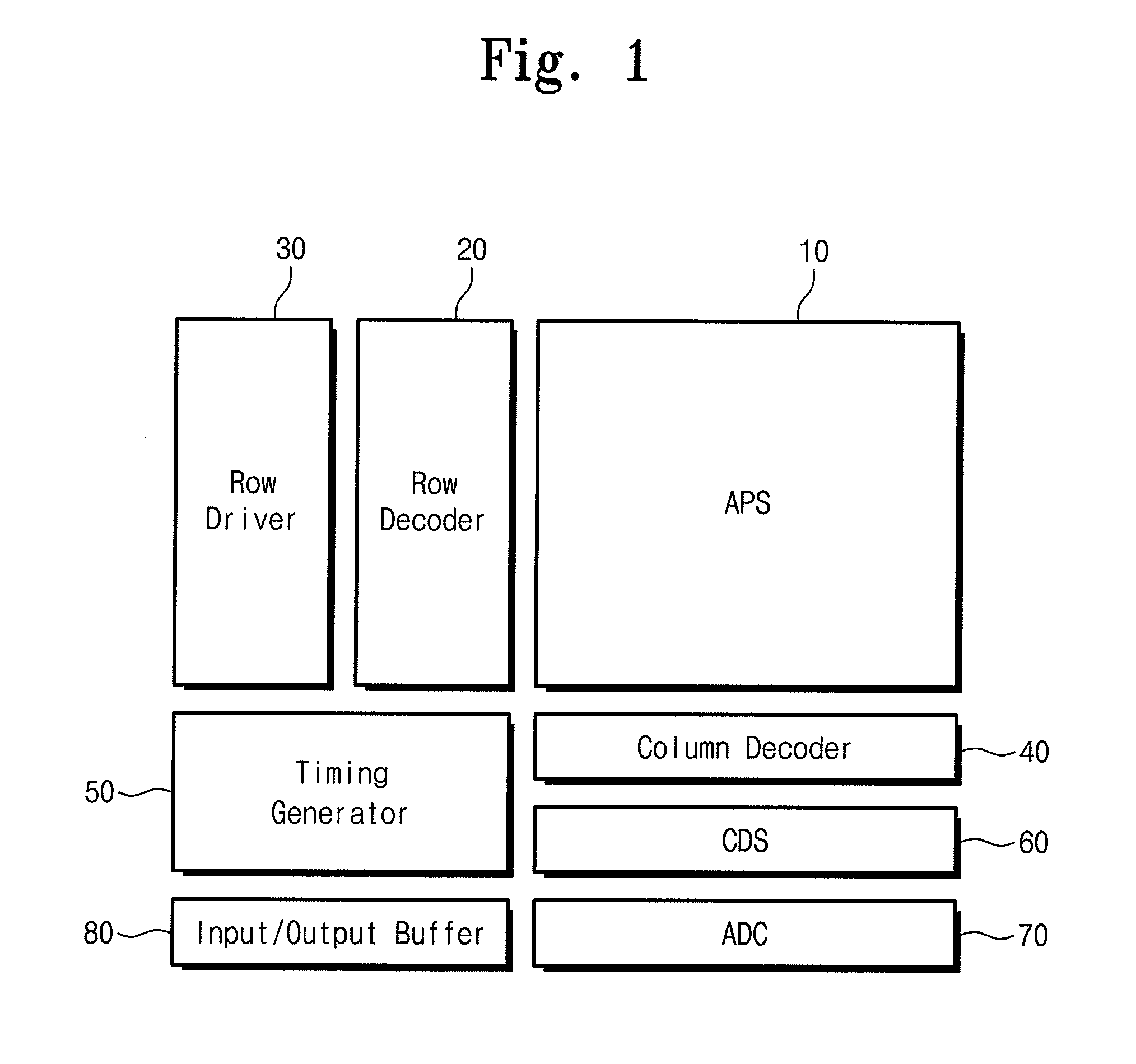
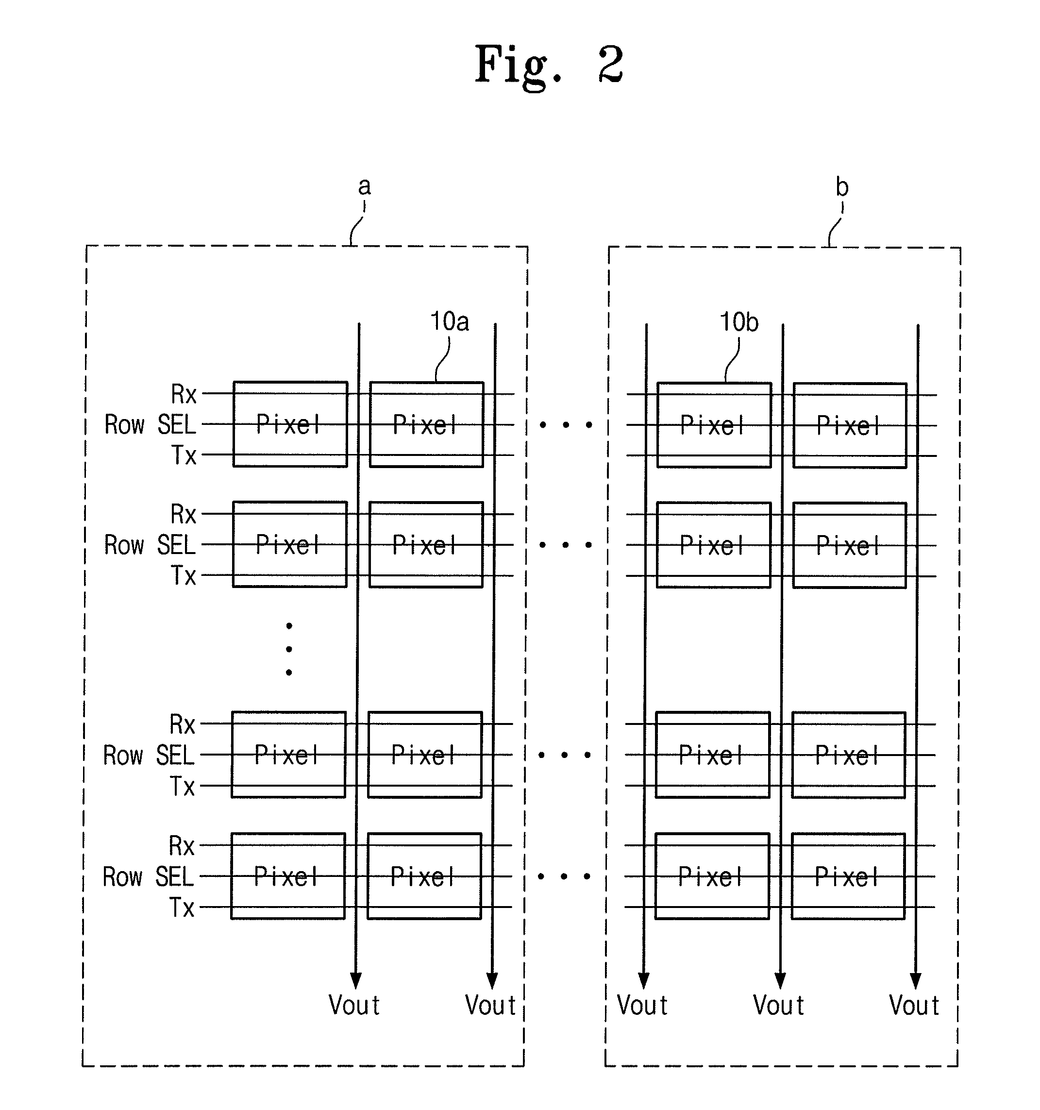
[0028]FIG. 1 is a block diagram of an image sensor in accordance with embodiments of the inventive concept. FIG. 2 is a circuit diagram of APS array of an image sensor in accordance with embodiments of the inventive concept.

[0029]Referring to FIG. 1, an image sensor in accordance with embodiments of the inventive concept may include, for example, an active pixel sensor (APS) array 10, a row decoder 20, a row driver 30, a column decoder 40, a timing generator 50, a correlated double sampler (CDS) 60,...


PUM


Abstract

Provided are an image sensor and a package including the same. The image sensor may include an interconnection layer comprising a plurality of interconnections that are vertically stacked, a light penetration layer including color filters and microlenses, a semiconductor layer disposed between the interconnection layer and the light penetration layer and including photoelectrical transformation elements and a light shielding pattern disposed between the light penetration layer and the semiconductor layer. A surface of the semiconductor layer adjacent to the light penetration layer defines a recess region recessed toward the interconnection layer. The light shielding pattern is formed in the recess region and at least one of the photoelectrical transformation elements is formed in the semiconductor layer between the light shielding pattern and the interconnection layer.

Description

CROSS-REFERENCE TO RELATED APPLICATIONS[0001]This U.S. non-provisional patent application claims priority under 35 U.S.C. §119 to Korean Patent Application No. 10-2010-0062509, filed on Jun. 30, 2010, the entire disclosure of which is hereby incorporated by reference herein in it's entirety.BACKGROUND[0002](i) Technical Field[0003]The present disclosure herein relates to image sensors and packages including the same, and more particularly, to an image sensor including a light shielding pattern and a package including the same.[0004](ii) Description of the Related Art[0005]An image sensor may convert an optical image to an electric signal. With the recent developments in the computer industry and the communication industry, an image sensor having increased performance is being increasingly required in various fields and products such as, for example, a digital camera, a camcorder, a personal communication system (PCS), a game machine, a security camera, a medical micro camera, etc.[0...

Claims


Application Information

Patent Timeline
Patent Type & Authority Applications(United States)
IPC IPC(8): H01L31/0232
CPCH01L27/14618H01L27/14623H01L27/14687H01L27/1464H01L27/14685H01L27/14632H01L2924/0002H01L2924/00H01L27/146H04N25/00
Inventor YOON, JUNHO
Owner SAMSUNG ELECTRONICS CO LTD
Why Eureka
Try Eureka