Semiconductor package having a stacked structure

a technology of semiconductor chips and stacked structures, which is applied in the direction of semiconductor devices, semiconductor/solid-state device details, electrical apparatus, etc., can solve the problems of increased number of semiconductor chips stacked within the package, defects thereon, etc., and achieve excellent production yield, effective dispersion pressure, and high capacity memory

Active Publication Date: 2012-01-05
SAMSUNG ELECTRONICS CO LTD
View PDF3 Cites 19 Cited by
  • Summary
  • Abstract
  • Description
  • Claims
  • Application Information

AI Technical Summary

Benefits of technology

[0006]Embodiments of the inventive concept provide a semiconductor package with a high capacity memory and excellent production yield by effectively dispersing pressure when stacking a plurality of semiconductor chips.
[0007]Embodiments of the inventive concept also provide an electronic system including a semiconductor package with a high capacity memory and excellent production yield.

Problems solved by technology

However, as the semiconductor chips become light and thin, the number of semiconductor chips which are stacked within the package is increased.
Accordingly, due to an increase in overhang area, fabrication processes such as warpage or cracks in the semiconductor chip have caused defects thereon.

Method used


Image

  • Semiconductor package having a stacked structure
  • Semiconductor package having a stacked structure
  • Semiconductor package having a stacked structure

Examples


second embodiment

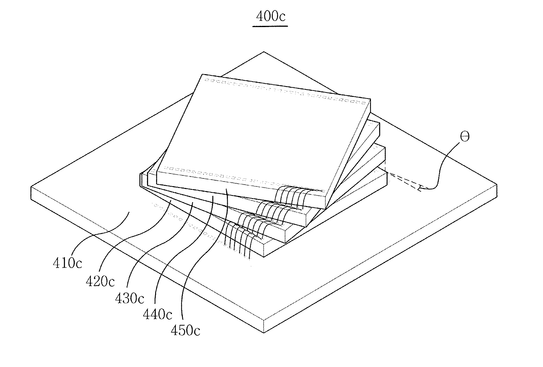
[0080]FIG. 4 is a cross-sectional view of a semiconductor package according to another embodiment of the present general inventive concept. Referring to FIG. 4, a semiconductor package 200 may include a substrate 210, a first semiconductor chip 220 stacked on the substrate 210 and a second semiconductor chip 230 stacked on the first semiconductor chip 220. The first semiconductor chip 220 is stacked on the substrate 210. The second semiconductor chip 230 is stacked on the first semiconductor chip 220.

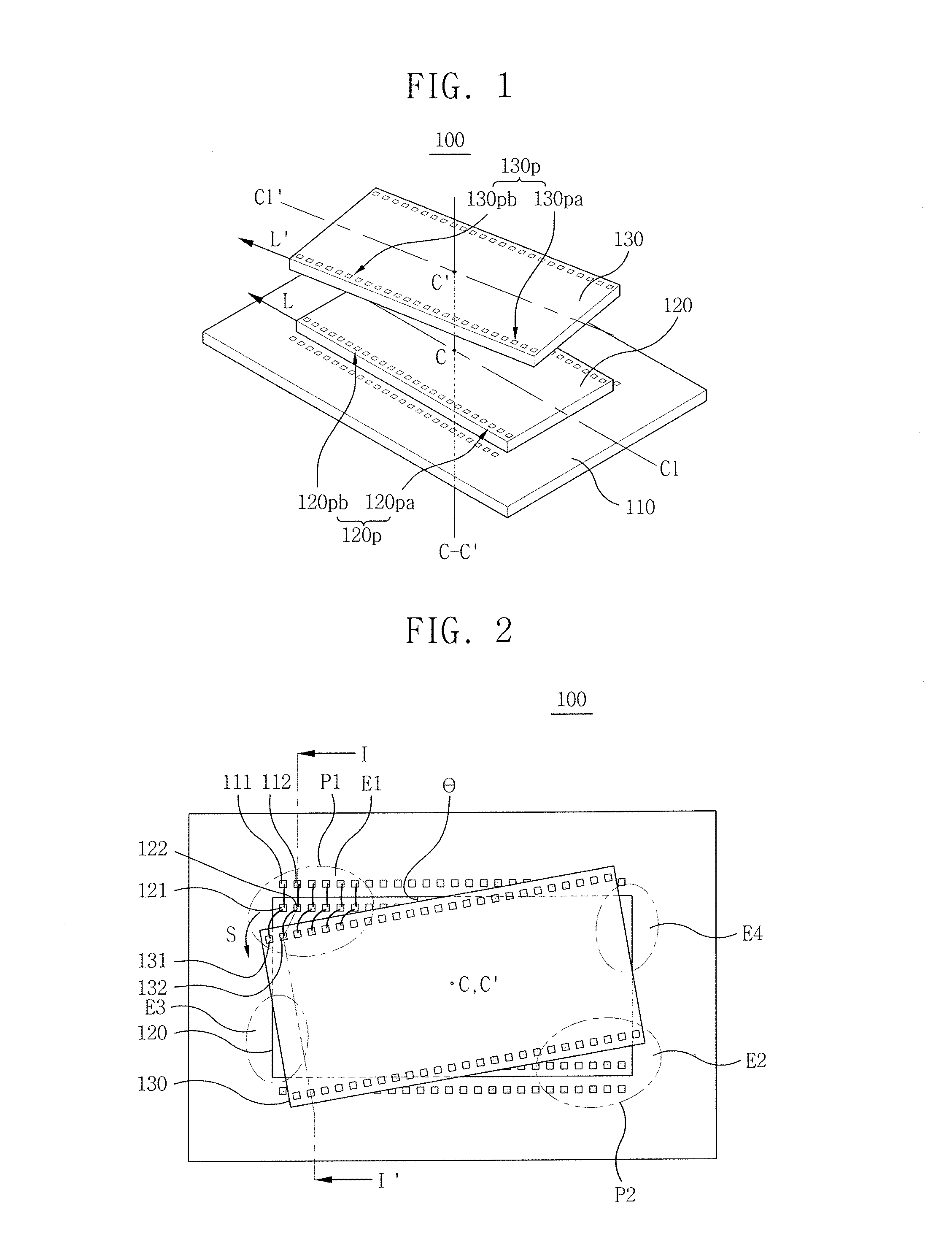
[0081]Herein, the second semiconductor chip 230 is rotated by an angle about a rotation axis, for example, a virtual center axis C-C′ which connects a center C of the first semiconductor chip 220 and a center C′ of the second semiconductor chip 230 to be stacked on the first semiconductor chip 220. The virtual center axis C-C′ connecting the centers C and C′ may be a stack direction of the semiconductor chips 220 and 230 and may be perpendicular to the substrate 210. As illustrated in F...


PUM


Abstract

A semiconductor package includes a substrate, a first semiconductor chip stacked on the substrate and a second semiconductor chip stacked on the first semiconductor chip. In the semiconductor package, the second semiconductor chip is rotated to be stacked on the first semiconductor chip. The semiconductor package is used in an electronic system.

Description

CROSS-REFERENCE TO RELATED APPLICATIONS[0001]This application claims priority under 35 U.S.C. §119 to Korean Patent Application No. 10-2010-0063931 filed on Jul. 2, 2010, the disclosure of which is hereby incorporated by reference in their entirety.BACKGROUND OF THE INVENTION[0002]1. Field of the Invention[0003]Embodiments of the inventive concept relate to a semiconductor package including stacked semiconductor chips and an electronic system including the semiconductor package.[0004]2. Description of the Related Art[0005]Semiconductor packages are configured to electrically connect a plurality of semiconductor chips with each other in a package. However, as the semiconductor chips become light and thin, the number of semiconductor chips which are stacked within the package is increased. Accordingly, due to an increase in overhang area, fabrication processes such as warpage or cracks in the semiconductor chip have caused defects thereon.SUMMARY OF THE INVENTION[0006]Embodiments of t...

Claims


Application Information

Patent Timeline
Patent Type & Authority Applications(United States)
IPC IPC(8): H01L23/52
CPCH01L23/3121H01L24/05H01L24/06H01L24/16H01L24/29H01L24/32H01L24/48H01L24/49H01L25/0657H01L2224/05611H01L2224/05613H01L2224/05616H01L2224/05639H01L2224/05644H01L2224/05647H01L2224/05655H01L2224/05669H01L2224/06155H01L2224/16145H01L2224/16225H01L2224/2919H01L2224/32145H01L2224/32225H01L2224/45124H01L2224/45144H01L2224/48145H01L2224/48225H01L2224/49175H01L2224/73265H01L2225/06506H01L2225/0651H01L2225/06562H01L2924/1434H01L2924/1438H01L2924/15311H01L2924/01079H01L2224/48644H01L2224/48647H01L2224/48655H01L2224/48669H01L2224/48611H01L2224/48616H01L2224/48639H01L2224/48711H01L2224/48739H01L2224/48747H01L2224/48755H01L2224/48769H01L2224/48716H01L2924/01013H01L2924/01028H01L2224/48091H01L2224/0401H01L2224/05554H01L2924/00H01L2924/3512H01L2224/48744H01L2224/48713H01L2224/48613H01L2924/00012H01L2224/48227H01L2924/00014H01L2924/15787H01L2924/181H01L24/73H01L2924/10161H01L2224/45099
Inventor LEE, JIN-YANGHAN, CHAN-MINKIM, KIL-SOO
Owner SAMSUNG ELECTRONICS CO LTD
Why Eureka
Try Eureka