Display device

a display device and display screen technology, applied in the field of display devices, can solve the problems of emi generation, adverse effects on the operation of other electronic devices inside and outside the display device, and emi generation in the display screen, so as to save the power of the liquid crystal display device and prevent a malfunction

Active Publication Date: 2012-01-12
JAPAN DISPLAY INC +2
View PDF6 Cites 4 Cited by
  • Summary
  • Abstract
  • Description
  • Claims
  • Application Information

AI Technical Summary

Benefits of technology

[0006]The above-mentioned charge sharing driving plays an important role in saving power of the liquid crystal display device. It has been revealed, however, that electro magnetic interference (EMI) is generated from the liquid crystal display screen during the charge sharing driving. If the EMI increases, the operations of other electronic devices inside and outside the display device may be adversely affected. Particularly in a touch panel type liquid crystal display device, which operates as an input device when a finger or the like of the user contacts the screen, the electronic devices are arranged in proximity to the liquid crystal display screen and accordingly vulnerable to the influence of the EMI generated in the display screen. It is therefore necessary to prevent a malfunction caused by an erroneous recognition of position coordinates.
[0007]The present invention has been made in view of the above-mentioned circumstances, and it is therefore an object thereof to provide a driver circuit for controlling supply of charges to an array of cells capable of storing the charges, in which EMI generated in charge sharing driving of the charges can be reduced.

Problems solved by technology

It has been revealed, however, that electro magnetic interference (EMI) is generated from the liquid crystal display screen during the charge sharing driving.
If the EMI increases, the operations of other electronic devices inside and outside the display device may be adversely affected.
Particularly in a touch panel type liquid crystal display device, which operates as an input device when a finger or the like of the user contacts the screen, the electronic devices are arranged in proximity to the liquid crystal display screen and accordingly vulnerable to the influence of the EMI generated in the display screen.

Method used


Image

  • Display device
  • Display device
  • Display device

Examples


first embodiment

[0035]Now, a brief summary of charge sharing driving of the present invention and the present invention are described with reference to FIGS. 1 to 11.

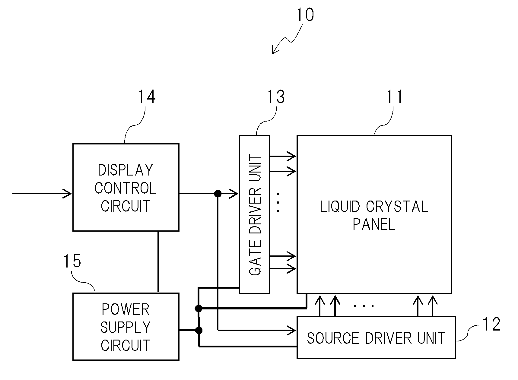
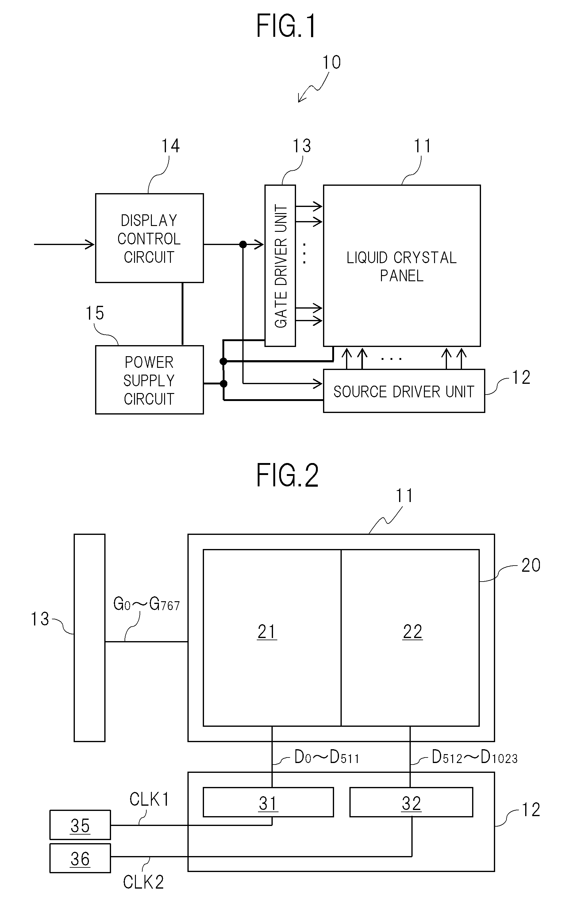
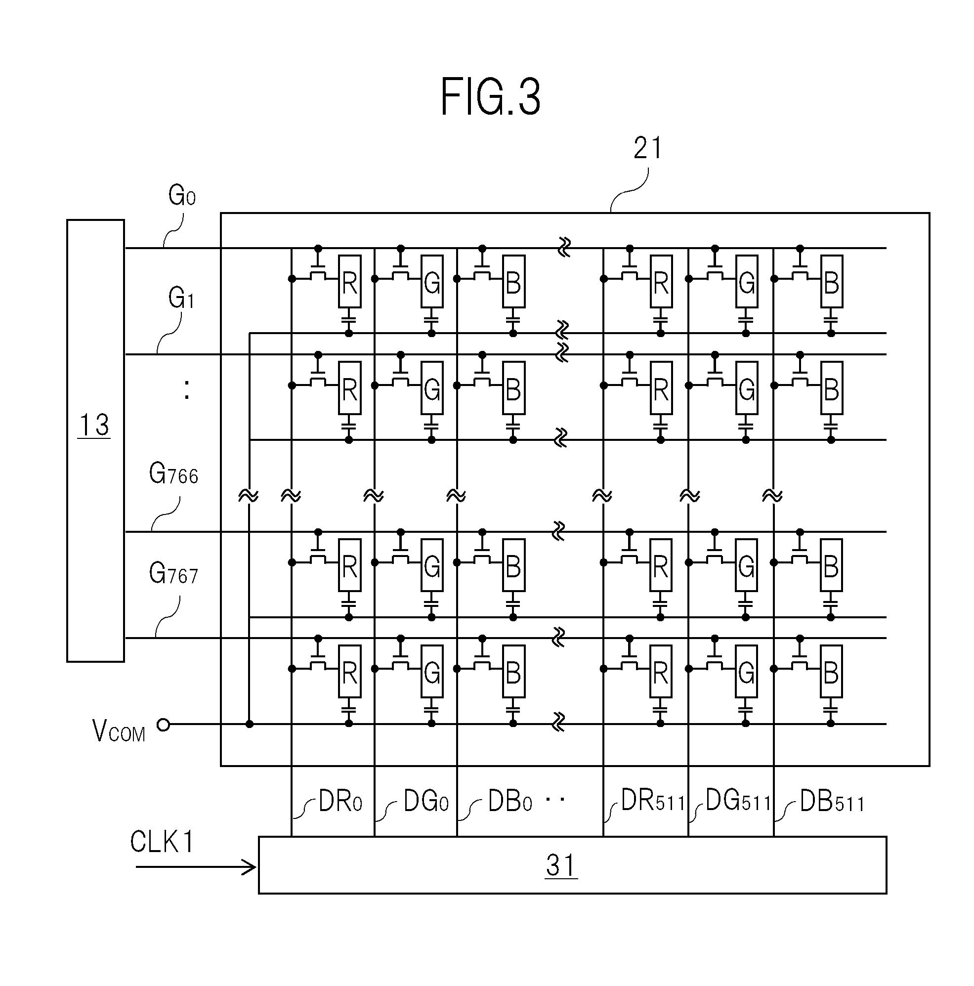
[0036]FIG. 1 schematically illustrates a configuration of a thin film transistor (TFT) liquid crystal display device 10 including a driver circuit according to a first embodiment of the present invention. The liquid crystal display device 10 includes: (a) a liquid crystal panel 11 including TFTs, for operating the TFTs to display an image visually; (b) a source driver unit 12 for controlling a voltage to be applied to a drain terminal of the TFT included in the liquid crystal panel 11; (c) a gate driver unit 13 for controlling a voltage to be applied to a gate terminal of the TFT included in the liquid crystal panel 11; (d) a display control circuit 14 for receiving image data to be displayed and instructing operations of the source driver unit 12 and the gate driver unit 13; and (e) a power supply circuit 15 for supplying power to the...

second embodiment

[0051]Hereinafter, the present invention is described with reference to FIG. 13.

[0052]A liquid crystal display device according to the second embodiment has the same configuration as that of the liquid crystal display device of the first embodiment except that the internal configuration of the driving section 231 of FIG. 11 is different, and hence description thereof is omitted. FIG. 13 is a diagram schematically illustrating an internal configuration of a driving section 331 corresponding to the driving section 231 of the first embodiment. Referring to FIG. 13, drain signals DR0, DG0, DB0, DR1, and DG1 are connected to a DR0 circuit 311, a DG0 circuit 312, a DB0 circuit 313, a DR1 circuit 314, and a DG1 circuit 315, and also connected to a common line CL via a switch SW321, a switch SW322, a switch SW323, a switch SW324, and a switch SW325, respectively. In other words, in FIG. 12 of the first embodiment, the switches SW221 to SW223 for setting the pair of two adjacent lines to the...

third embodiment

[0056]Hereinafter, the present invention is described with reference to FIG. 14.

[0057]A liquid crystal display device according to the third embodiment has the same configuration as that of the liquid crystal display device of the first embodiment except that the internal configuration of the driving section 231 of FIG. 11 is different, and hence description thereof is omitted. FIG. 14 is a diagram schematically illustrating an internal configuration of a driving section 431 corresponding to the driving section 231 of the first embodiment. Referring to FIG. 14, drain signals DR0, DG0, DB0, and DR1 are connected to a DR0 circuit 411, a DG0 circuit 412, a DB0 circuit 413, and a DR1 circuit 414, and also connected to a common line CL via a switch SW421, a switch SW422, a switch SW423, and a switch SW424, respectively. Further, the driving section 431 is divided into a plurality of unit driving sections, each of which is formed for each line (e.g., a unit driving section constituted by ...


PUM


Abstract

Provided is a display device including a driver circuit for controlling supply of charges to an array of cells capable of storing the charges. In the driver circuit, a preceding electrically connecting part (SW221) controlled by a clock signal (CLK1) electrically connects an output signal line of a first circuit (211) having a positive polarity which is a potential higher than a reference potential and an output signal line of a second circuit (212) having a negative polarity which is a potential lower than the reference potential. After a predetermined time period has elapsed, a subsequent electrically connecting part (SW222) controlled by a clock signal (CLK2) electrically connects an output signal line of a third circuit (213) having the positive polarity and an output signal line of a fourth circuit (214) having the negative polarity.

Description

CROSS-REFERENCE TO RELATED APPLICATION[0001]The present application claims priority from Japanese application JP 2010-156052 filed on Jul. 8, 2010, the content of which is hereby incorporated by reference into this application.BACKGROUND OF THE INVENTION[0002]1. Field of the Invention[0003]The present invention relates to a display device, and more specifically, to a display device using a driver circuit for controlling supply of charges to an array of cells capable of storing the charges, such as a liquid crystal display panel, an organic electroluminescence (EL) panel, and a dynamic random access memory (DRAM).[0004]2. Description of the Related Art[0005]Liquid crystal display devices are widely used as display devices for information communication terminals, such as computers, and television sets. The liquid crystal display device is a device in which the alignment of liquid crystal molecules which are sealed between two substrates is changed to change the transmittance of light,...

Claims


Application Information

Patent Timeline
Patent Type & Authority Applications(United States)
IPC IPC(8): G09G5/00
CPCG09G3/3614G09G3/3666G09G2330/06G09G2310/0213G09G2300/0426
Inventor MISONOU, TOSHIKIYAMAGISHI, YASUHIKO
Owner JAPAN DISPLAY INC
Why Eureka
Try Eureka