Measurement method for measuring shape of test surface, measurement apparatus, and method for manufacturing optical element

Inactive Publication Date: 2012-01-19
CANON KK
View PDF2 Cites 20 Cited by
  • Summary
  • Abstract
  • Description
  • Claims
  • Application Information

AI Technical Summary

Benefits of technology

[0009]According to an aspect of the present invention, a measurement method and measurement app

Problems solved by technology

Since the reference lens needs to be larger than the lens to be measured and also needs to have a surface proce

Method used


Image

  • Measurement method for measuring shape of test surface, measurement apparatus, and method for manufacturing optical element
  • Measurement method for measuring shape of test surface, measurement apparatus, and method for manufacturing optical element
  • Measurement method for measuring shape of test surface, measurement apparatus, and method for manufacturing optical element

Examples


embodiments

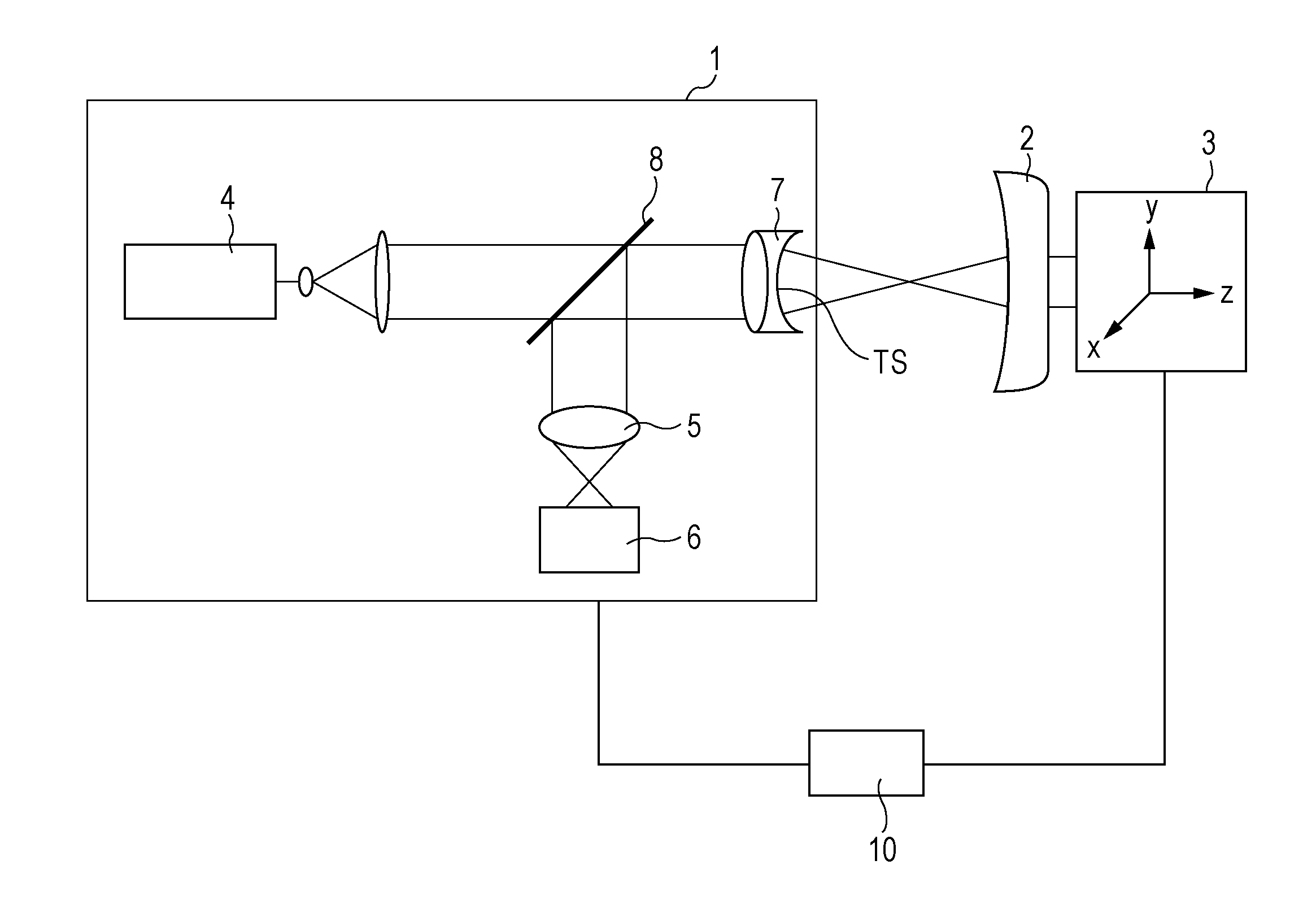
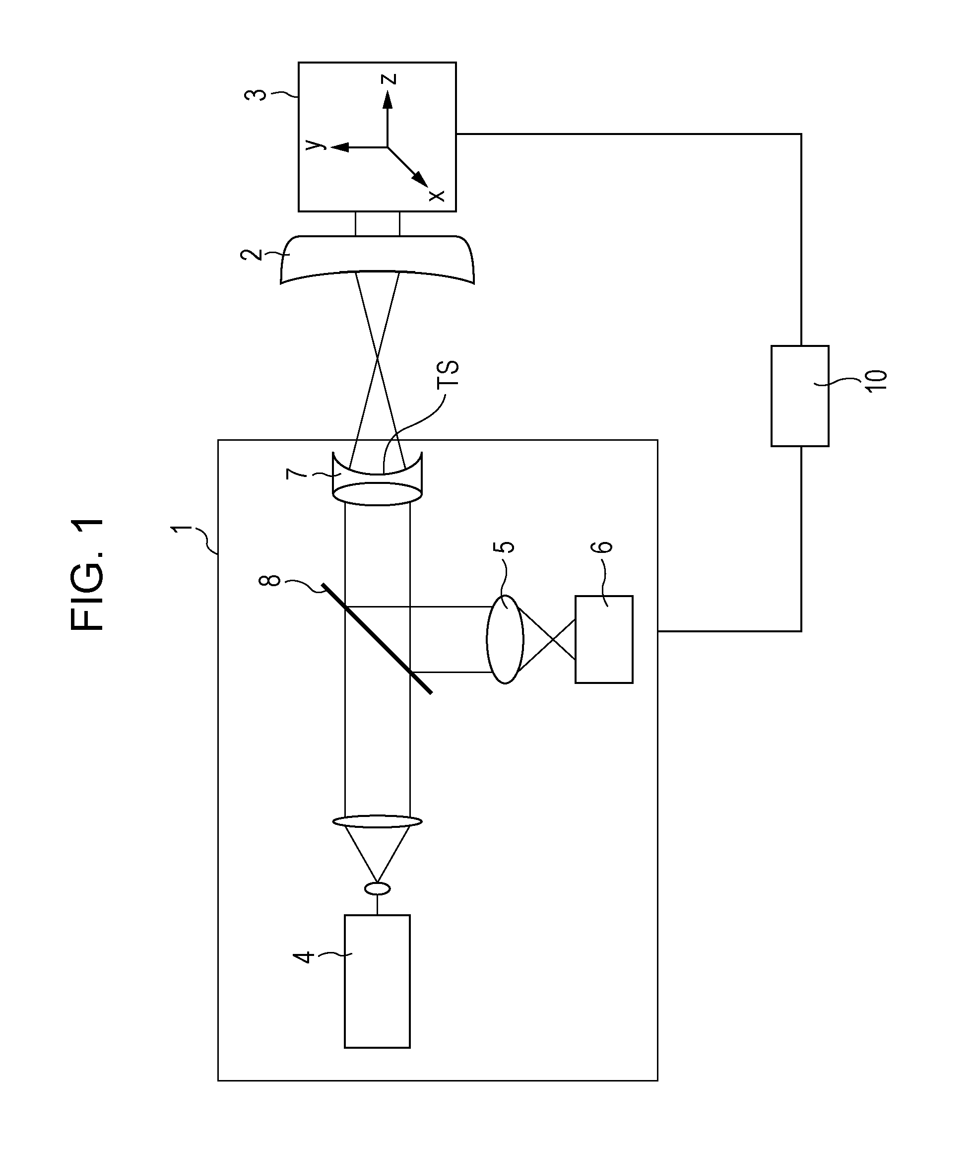
[0033]FIG. 1 illustrates a measurement apparatus that measures the shape of a test surface. The measurement apparatus includes an interferometer 1, a stage 3 that supports a test object 2, and a control unit 10 that controls the interferometer 1 and the stage 3. An interferometer is an apparatus (measurement unit) that causes the reference wavefront and the test wavefront to interfere with each other and that measures interference fringes. The interferometer 1 illustrated in FIG. 1 is a Fizeau interferometer. The test object 2 is supported by the stage 3, and is made to move in the x, y, and z directions or to rotate about the x, y, and z axes.

[0034]The interferometer 1 mainly includes a laser (light source) 4, a lens 5, a sensor 6, a TS lens 7, and a beam splitter 8. Light emitted from the laser 4 is collimated by a lens, and enters the TS lens 7 through the beam splitter 8. The TS lens 7 splits the light from the laser 4 into reflected light and transmitted light on a surface TS (...

embodiment 2

[0082]In this embodiment, resolutions are changed by setting pixels used for photographing performed by an image pickup element.

[0083]Measurement ranges on a test surface will be described with reference to FIG. 12. The thick line illustrated in FIG. 12 represents the outer periphery of the test surface, and dotted line circles C1 to C7 represent respective measurement ranges. In this example, the test surface is divided into seven measurement ranges and is measured. Each of C1 to C7 partially overlaps at least another measurement range, and an overlap region is formed. The regions (areas or diameters) of C1 to C7 are the same.

[0084]In FIG. 12, the test object is an aspherical shaped lens with rotational symmetry, and it is assumed that the region C1 (central portion) has a different amount of asphericity from the regions C2 to C7 (peripheral portions) while all the regions C2 to C7 have an equal amount of asphericity. Thus, the center portion, i.e., C1 (first measurement range), an...

embodiment 3

[0092]In this embodiment, binning conditions under which a CCD reads signals of pixels are changed. Binning is a function for combining several adjacent pixels on a CCD into a group to virtually increase the area of a light receiving surface so that the electrical signals can be amplified and detected. Binning allows the same effect as when the number of pixels is reduced to be obtained. Binning is generally represented as, for example, 1×1, 2×2, 3×3, . . . Binning 1×1 means that each pixel is used as it is. Binning 2×2 means that a pixel region of 2 pixels×2 pixels=4 pixels is integrated into one large pixel. Here, since the pixel size is increased to be four times the original, the sensitivity to light also becomes four times the original but the resolution becomes half the original. Therefore, if a 2048×2048 CCD is used, 2×2 binning provides 1024×1024 pixel resolution, resulting in low-resolution measurement.

[0093]According to this embodiment, high-resolution measurement is perfo...


PUM


Abstract

Provided is a measurement method or apparatus that can reduce the time for measuring the shape of an entire test surface. Each of a plurality of measurement ranges is set so that one measurement range overlaps a portion of at least another measurement range to form an overlap region, each measurement range being a portion of the test surface. Then, the shape of the test surface is measured at a first resolution in a first measurement range among the plurality of measurement ranges, and is measured at a second resolution in a second measurement range. Pieces of data of the shapes of the test surface in the plurality of measurement ranges are stitched together using the resulting measurement data to calculate the shape of the test surface.

Description

TECHNICAL FIELD[0001]The present invention relates to a measurement method for measuring the shape of a test surface, a measurement apparatus, and a method for manufacturing an optical element.BACKGROUND ART[0002]Lenses with a large aperture diameter that is more than a diameter of 200 mm are used in high-magnification zoom lenses. In order to measure the surface shape of such lenses or the wavefront of light from the lenses, an interferometer with a large aperture diameter, as a measurement apparatus, and a reference lens used in the interferometer are necessary. Since the reference lens needs to be larger than the lens to be measured and also needs to have a surface processed with high accuracy, it is difficult to manufacture the reference lens, and much cost and time are required.[0003]Thus, a technique for measuring a test surface using a plurality of smaller measurement ranges has been used (see PTL 1). This method computes data of the shape of an entire test surface by acquiri...

Claims


Application Information

Patent Timeline
IPC IPC(8): G01B11/02G01B11/24
CPCG01B2210/52G01M11/0271G01M11/025G01M11/005
Inventor OSAKI, YUMIKO
Owner CANON KK
Why Eureka
Try Eureka