Modification of logic by morphological manipulation of a semiconductor resistive element

a resistive element and logic technology, applied in the field of electronic devices, can solve problems such as damage to electronic devices

Inactive Publication Date: 2012-02-09
AVAGO TECH WIRELESS IP SINGAPORE PTE
View PDF9 Cites 94 Cited by
  • Summary
  • Abstract
  • Description
  • Claims
  • Application Information

AI Technical Summary

Problems solved by technology

Various existing methods suffer from one or more deficiencies, such as damage to the electronic device (e.g. radiation-induced soft errors), a limited number of reconfiguration cycles that may be performed on the device, complex processing steps or exotic materials.

Method used


Image

  • Modification of logic by morphological manipulation of a semiconductor resistive element
  • Modification of logic by morphological manipulation of a semiconductor resistive element
  • Modification of logic by morphological manipulation of a semiconductor resistive element

Examples


Embodiment Construction

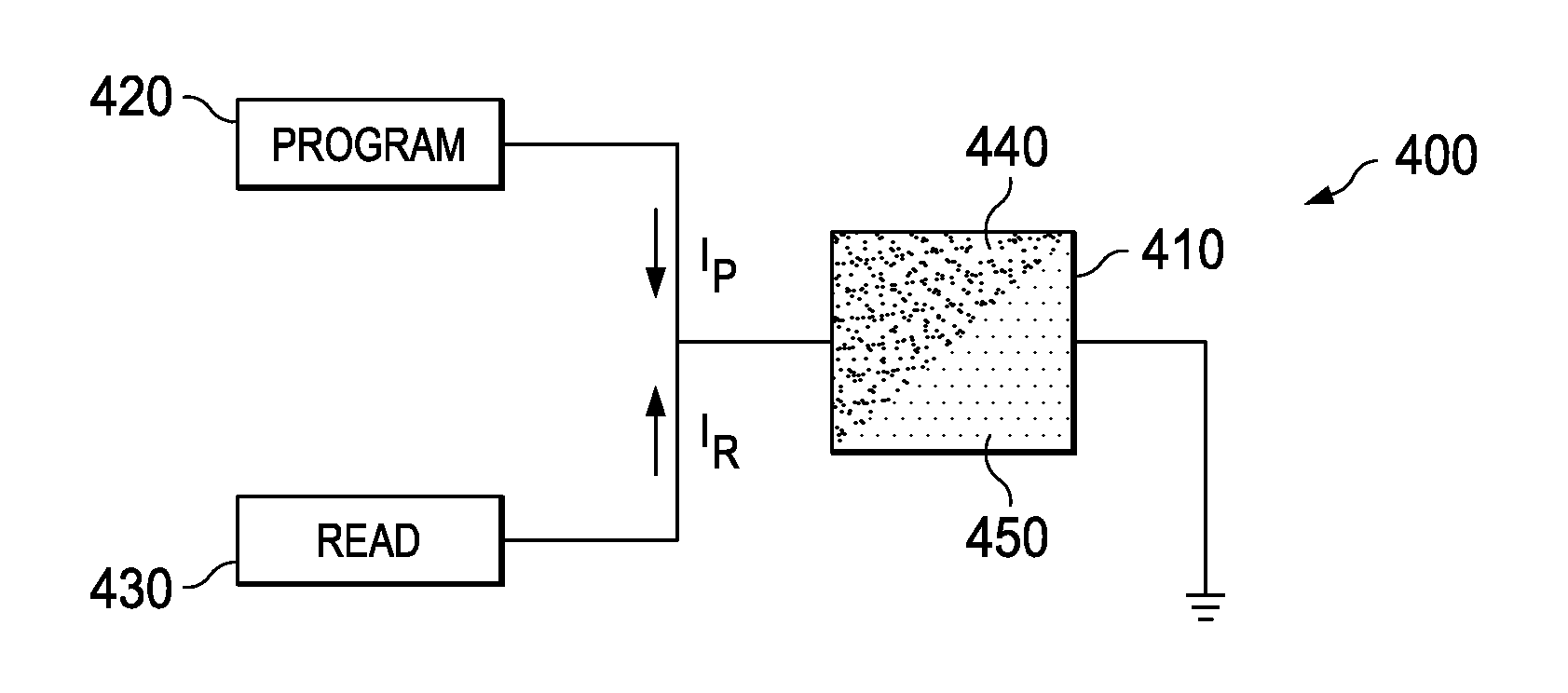
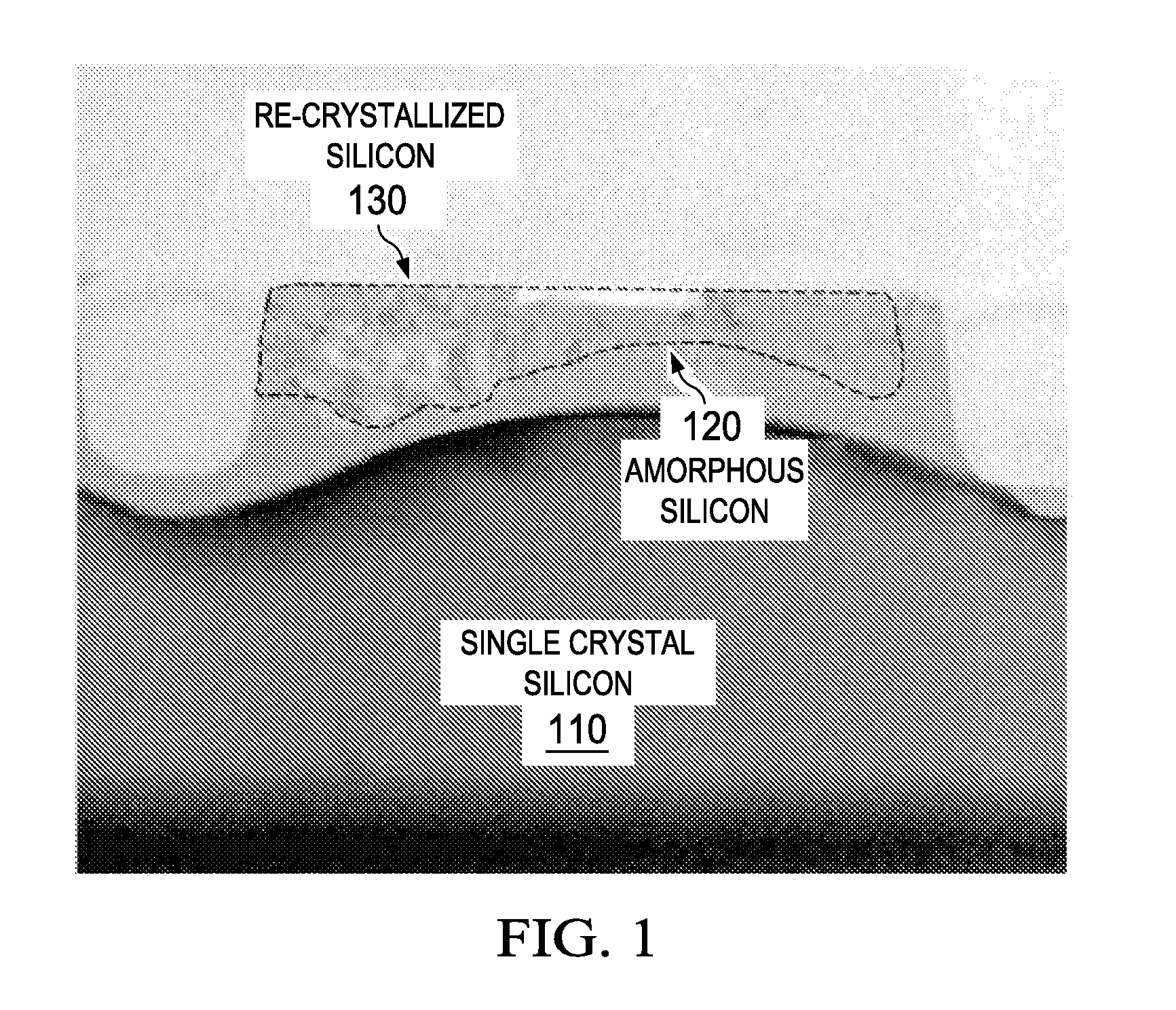
[0020]This disclosure benefits from the recognition that resistive properties of a semiconductor region in an electronic device may be beneficially modified to alter the operation of the electronic device. Such modification may include heating the semiconductor region to induce a change of morphology of the region. Unlike various conventional approaches, embodiments herein present methods that do not significantly damage the electronic device. Moreover, the properties of the semiconductor region may be reversibly changed. Thus, one or more operational characteristics of the electronic device may be changed from initial characteristics, and later restored to the initial characteristics or to yet another set of characteristics.

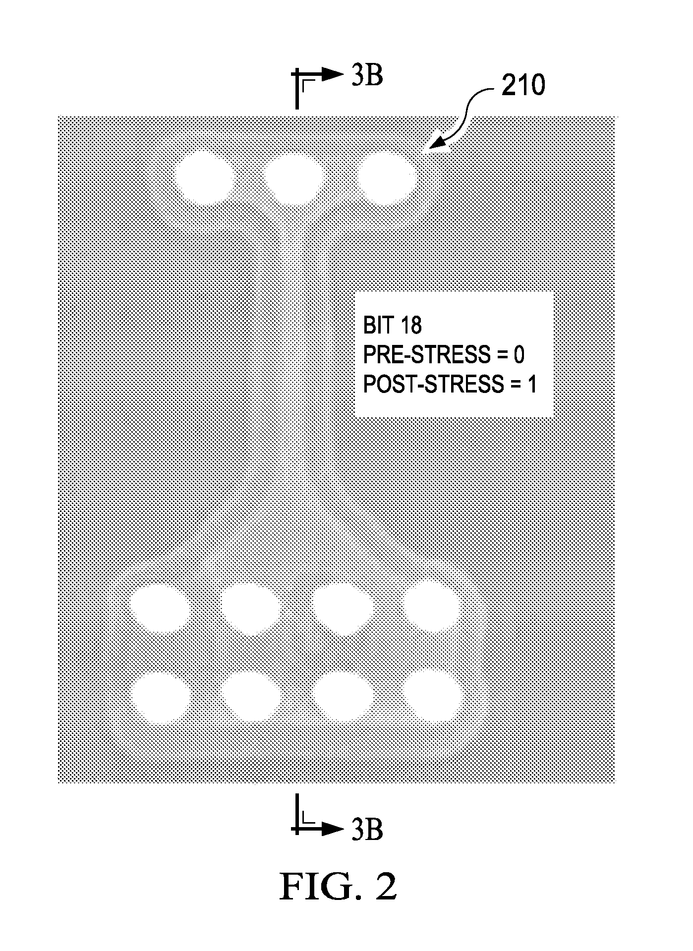
[0021]This disclosure provides in various embodiments an adjustable resistive element that may be switched between two or more distinct resistance values. As used herein, a resistive element has a continuous conductive path, e.g. the element is not blown to crea...


PUM

PropertyMeasurementUnit
fall timeaaaaaaaaaa
mean grain diameteraaaaaaaaaa
mean grain sizeaaaaaaaaaa

Abstract

An electronic device includes a substrate with a resistive element located thereover. The resistive element includes a semiconductor region. A read module is configured to determine a resistance of the resistive element. A programming module is configured to cause a current to flow through the semiconductor region. The current is sufficient to induce a change of morphology of at least a portion of the semiconductor region.

Description

[0001]This application is related to PCT Application No. PCT / US08 / 76976 filed by Frank A. Baiocchi, et al. on Sep. 19, 2008, entitled “Allotropic Change in Silicon Induced by Electromagnetic Radiation for Resistance Tuning of Integrated Circuits”, commonly assigned with this application and incorporated herein by reference; and co-pending U.S. patent application Ser. No. ______ (attorney docket number L09-0628US1) filed by John DeLucca, et al., entitled “Modification of Semiconductor Optical Paths by Morphological Manipulation”, commonly assigned with this application and incorporated herein by reference.TECHNICAL FIELD[0002]This application is directed, in general, to an electronic device and, more specifically, to reconfiguring an operation thereof.BACKGROUND[0003]In some circumstances it is desirable to reconfigure an operational aspect of an electronic device. Such reconfiguration may be for the purpose, e.g., of storing information, or changing a function provided by the device...

Claims


Application Information

Patent Timeline
Patent Type & Authority Applications(United States)
IPC IPC(8): G11C11/00H05K3/36
CPCG11C11/5678G11C13/0004G11C13/0069G11C2013/0073Y10T29/49126G11C2213/33G11C2213/56G11C2213/77G11C2013/0092
Inventor DELUCCA, JOHN M.CARGO, JAMESBAIOCCHI, FRANK A.
Owner AVAGO TECH WIRELESS IP SINGAPORE PTE
Why Eureka
Try Eureka