

Camera module
a camera module and module technology, applied in the field of camera modules, can solve the problems of increasing difficulty in finding an appropriate amount of lead soldering, and reducing the overall size of the camera modul
- Summary
- Abstract
- Description
- Claims
- Application Information
AI Technical Summary
Benefits of technology
Problems solved by technology
Method used
Image

Examples
Embodiment Construction
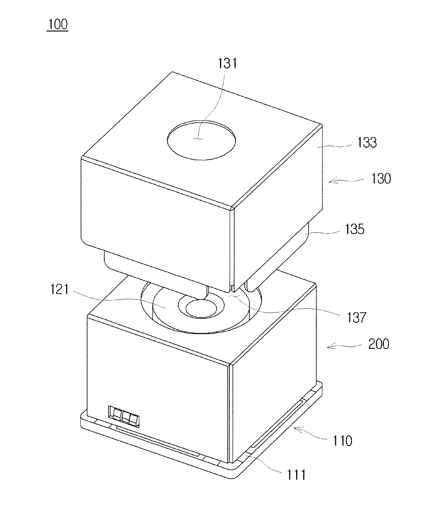
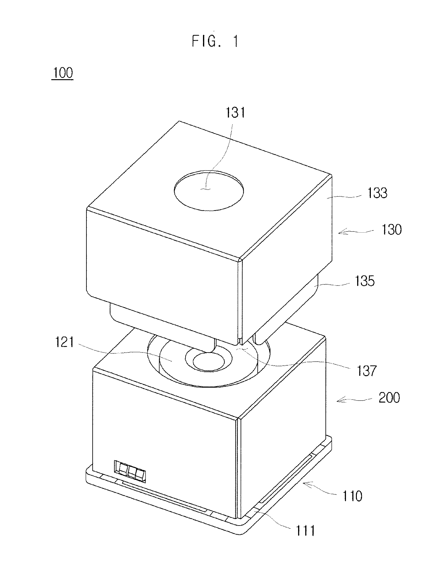
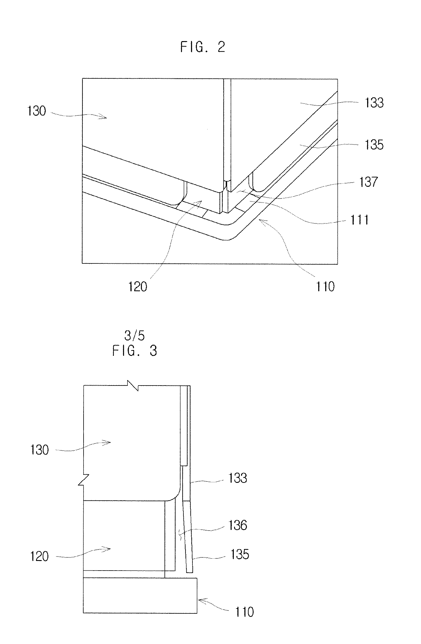
[0020]Since there can be a variety of permutations and embodiments of the present invention, certain embodiments will be illustrated and described with reference to the accompanying drawings. This, however, is by no means to restrict the present invention to certain embodiments, and shall be construed as including all permutations, equivalents and substitutes covered by the ideas and scope of the present invention. Throughout the description of the present invention, when describing a certain technology is determined to evade the point of the present invention, the pertinent detailed description will be omitted.
[0021]Terms such as “first” and “second” can be used in describing various elements, but the above elements shall not be restricted to the above terms. The above terms are used only to distinguish one element from the other.
[0022]The terms used in the description are intended to describe certain embodiments only, and shall by no means restrict the present invention. Unless cl...
PUM
 Abstract
Description
Claims
Application Information