Display apparatus having quantum dot layer

a display apparatus and quantum dot technology, applied in the field of display apparatuses, can solve the problems of reducing the output brightness of the display apparatus b>1/b> 67% of brightness, and achieve the effect of raising the luminescent efficiency of the display apparatus of the present invention

Inactive Publication Date: 2012-03-01
CHI LIN OPTOELECTRONICS CO LTD
View PDF2 Cites 50 Cited by
  • Summary
  • Abstract
  • Description
  • Claims
  • Application Information

AI Technical Summary

Benefits of technology

[0012]As a result, the color filter of prior art can be omitted. Compared with the luminescent efficiency of the display a...

Problems solved by technology

The disadvantage of the display apparatus 1 is that the color filter layer 15 filters some light so that the out...

Method used


Image

  • Display apparatus having quantum dot layer
  • Display apparatus having quantum dot layer
  • Display apparatus having quantum dot layer

Examples


Embodiment Construction

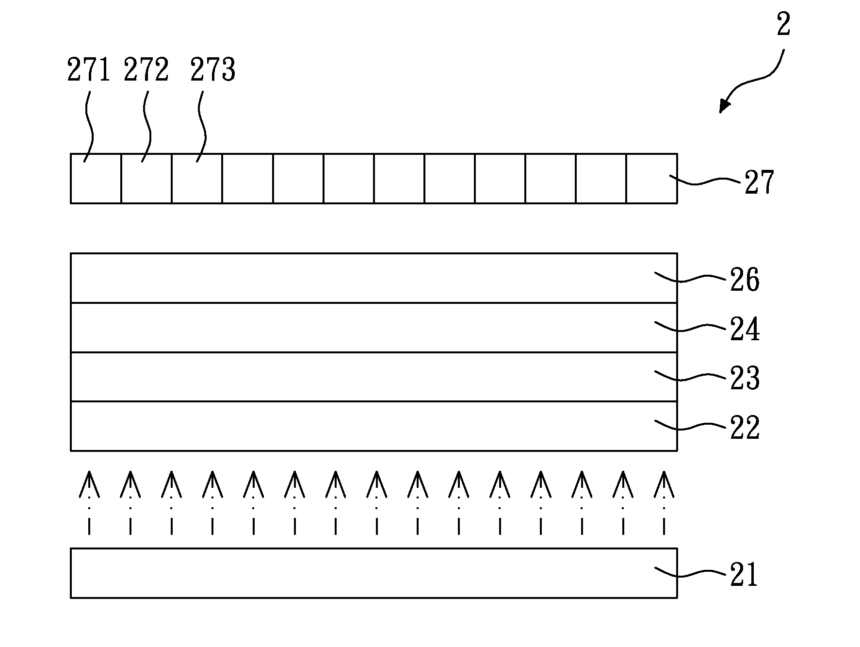
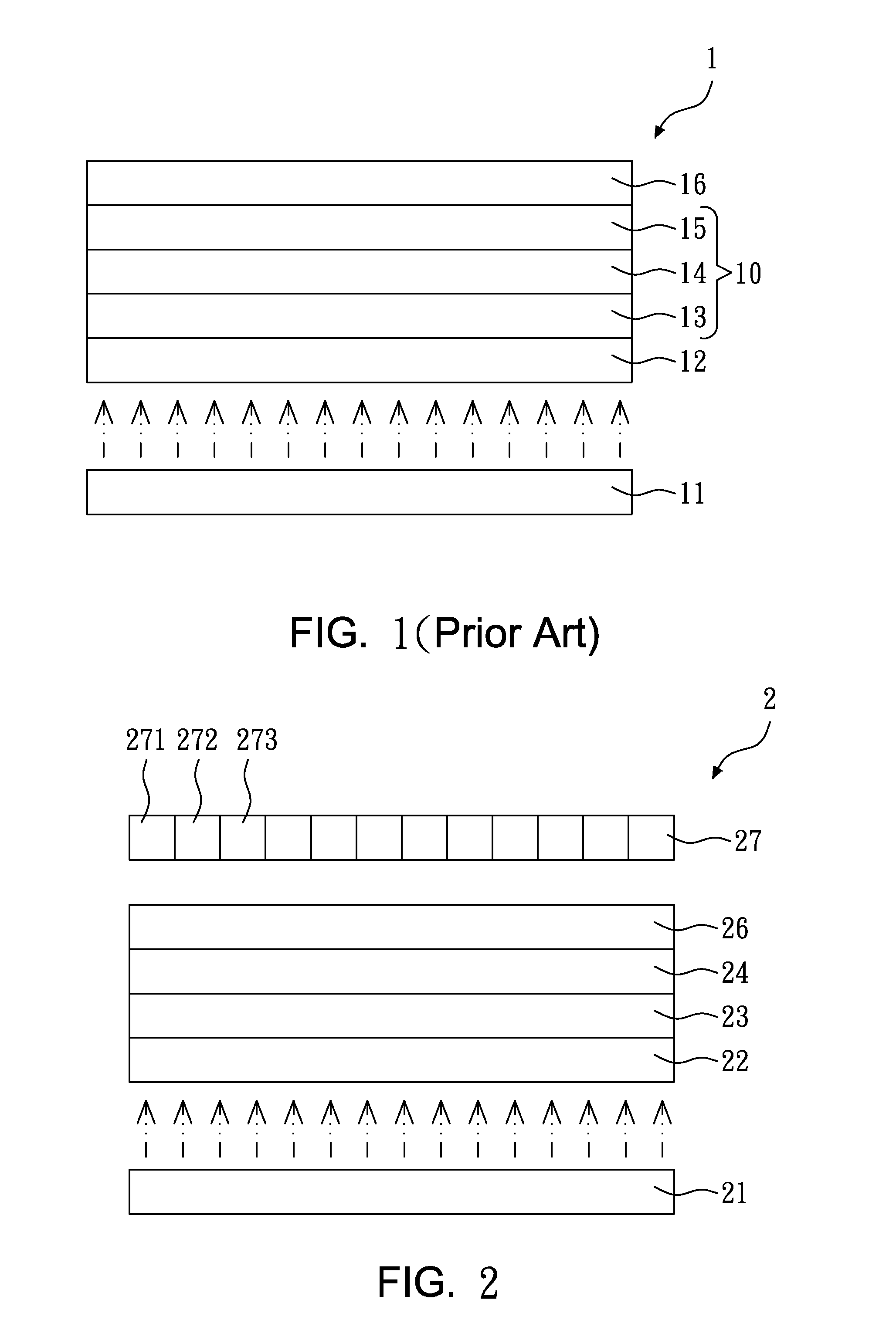
[0017]FIG. 2 shows a schematic view of a display apparatus according to a first embodiment of the present invention. The display apparatus 2 comprises a light source 21, a bottom polarizer 22, a thin film transistor (TFT) layer 23, a liquid crystal layer 24, a top polarizer 26 and a quantum dot layer 27. The light source 21, for example, at least one LED or CCFL, or a back light module, is used to provide a light beam. The bottom polarizer 22, the thin film transistor (TFT) layer 23, the liquid crystal layer 24, the top polarizer 26 and the quantum dot layer 27 are disposed above the light source 21 to display an image, and the image has a plurality of pixels. A PCB (not shown) is used for driving the thin film transistor (TFT) layer 23. The liquid crystal layer 24 has a plurality of liquid crystal molecules and is disposed on the thin film transistor (TFT) layer 23.

[0018]The thin film transistor (TFT) layer 23 has a plurality of TFTs arranged in a matrix. Each of the TFTs includes ...


PUM


Abstract

The present invention relates to a display apparatus, which has a quantum dot layer. The quantum dot layer has a plurality of quantum dot blocks which comprise quantum dots and are arranged in a matrix. The quantum dots when excited by the light convert the light wavelength so as to determine the color of each pixel of an image. As a result, the color filter of prior art can be omitted. Compared with the luminescent efficiency of the display apparatus of prior art, the luminescent efficiency of the display apparatus of the present invention can be raised.

Description

BACKGROUND OF THE INVENTION[0001]1. Field of the Invention[0002]The present invention relates to a display apparatus, and more particularly, to a display apparatus having a quantum dot layer.[0003]2. Description of the Related Art[0004]FIG. 1 shows a schematic view of a conventional display apparatus. The display apparatus 1 includes a light source 11, a bottom polarizer 12, a display panel 10, a top polarizer 16. The light source 11, for example, a plurality of LEDs or CCFLs, or a back light module, is used to provide a light beam. The display panel 10 includes a thin film transistor (TFT) layer 13, a liquid crystal layer 14 and a color filter layer 15. The display panel 10 is disposed above the light source 11 to display an image, and a PCB (not shown) is used for driving the display panel 10. The thin film transistor (TFT) layer 13 and the color filter layer 15 face with each other, and the liquid crystal layer 14 is disposed between the thin film transistor (TFT) layer 13 and th...

Claims


Application Information

Patent Timeline
IPC IPC(8): G02F1/1368H01L27/15B82Y20/00
CPCB82Y20/00G02F2001/01791H01L27/322G02F2202/107G02F1/133514G02F1/01791H10K59/38
Inventor SHIH, HSI-HSIN
Owner CHI LIN OPTOELECTRONICS CO LTD
Why Eureka
Try Eureka