Transistor structure, manufacturing method of transistor structure, and light emitting apparatus

a manufacturing method and transistor technology, applied in the direction of electrical equipment, semiconductor/solid-state device manufacturing, semiconductor devices, etc., can solve the problem of increasing manufacturing costs

Active Publication Date: 2012-03-15
SOLAS OLED LTD
View PDF4 Cites 12 Cited by
  • Summary
  • Abstract
  • Description
  • Claims
  • Application Information

AI Technical Summary

Benefits of technology

[0011]The present invention has been made in consideration of the above situation, and one of the main objects is to provide a transistor structure, a manufacturing method of a transistor structure and a light emitting apparatus in which a plurality of thin film transistors can be efficiently formed in a different configuration thin film transistors in different forms can be efficiently made and in which change of characteristic of each transistor by light emitted from a light emitting element and light from outside can be suppressed.

Problems solved by technology

Therefore, since each step for each thin film transistor is repeated, about twice as many steps than the normal process is necessary, and there is a problem that the increase in the number of steps results in an increase of manufacturing cost.

Method used


Image

  • Transistor structure, manufacturing method of transistor structure, and light emitting apparatus
  • Transistor structure, manufacturing method of transistor structure, and light emitting apparatus
  • Transistor structure, manufacturing method of transistor structure, and light emitting apparatus

Examples


first embodiment

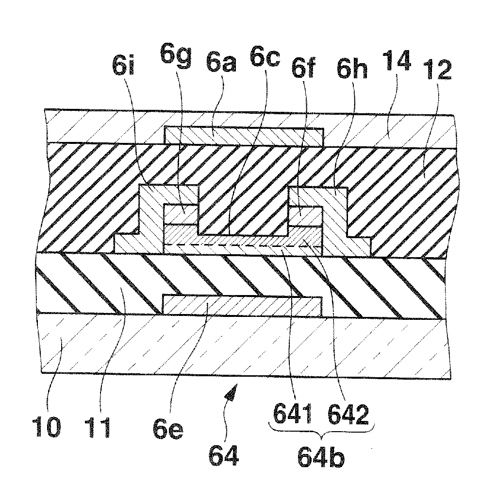
[0158]First, an EL panel and transistor structure of the first embodiment of the present invention is described.

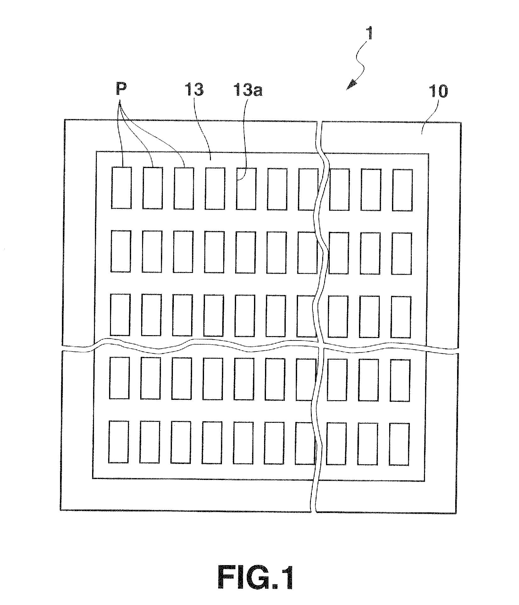
[0159]FIG. 1 is a planar view showing an arrangement structure of a plurality of pixels P in an EL panel 1 which is a light emitting apparatus.

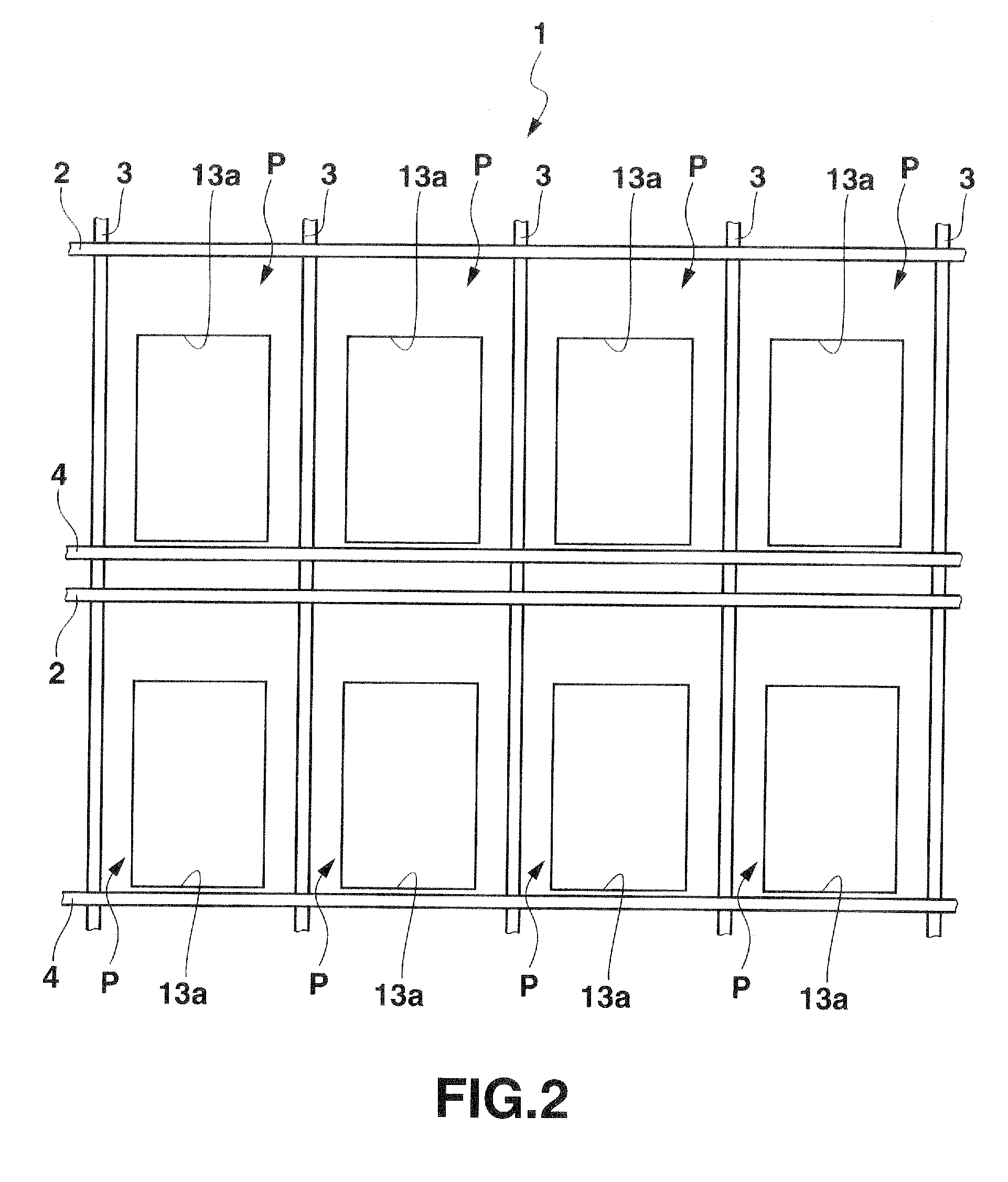
[0160]FIG. 2 is a planar view showing a schematic structure of the EL panel 1.

[0161]As shown in FIG. 1 and FIG. 2, a plurality of pixels P are arranged in a predetermined pattern in a matrix form on the EL panel 1. The plurality of pixels P include a red pixel P which emits light of R (red), green pixel P which emits light of G (green) and blue pixel P which emits light of B (blue).

[0162]On the EL panel 1, a plurality of scanning lines 2 are arranged along a row direction so as to be substantially parallel to each other, and a plurality of signal lines 3 are arranged along a column direction so as to be substantially parallel to each other and to be substantially orthogonal to the scanning lines 2 from a planar view.

[0163]Voltage su...

second embodiment

[0325]Next, the EL panel and the transistor structure of the second embodiment of the present invention are described. The same reference numerals are applied to the components which are similar to the above embodiment and the description is omitted.

[0326]Next, the configuration of the EL panel 1 of the second embodiment and the pixel P is described using FIG. 18 to FIG. 20.

[0327]FIG. 18 is a planar view corresponding to one pixel P of the EL panel 1 of the second embodiment.

[0328]FIG. 19 is a cross sectional view of a plane along arrows XIX-XIX shown in FIG. 18.

[0329]FIG. 20 is a cross sectional view of a plane along arrows XX-XX shown in FIG. 18.

[0330]FIG. 18 mainly shows electrodes and lines.

[0331]As shown in FIG. 18, each pixel P includes a transistor structure 562 including a switch transistor 52 and a driving transistor 62.

[0332]The switch transistor 52 and the driving transistor 62 each correspond to the switch transistor 5 and the driving transistor 6 shown in FIG. 3.

[0333]T...

third embodiment

[0438]Next, the EL panel and the transistor structure of the third embodiment of the present invention are described. The same reference numerals are applied to the components which are similar to the above embodiment and the description is omitted or simplified.

[0439]The configuration of the EL panel 1 of the third embodiment and the pixel P is described using FIG. 32 to FIG. 34.

[0440]FIG. 32 is a planar view corresponding to one pixel P of the EL panel 1 of the third embodiment.

[0441]FIG. 33 is a cross sectional view of a plane along arrows XXXIII-XXXIII shown in FIG. 32.

[0442]FIG. 34 is a cross sectional view of a plane along arrows XXXIV-XXXIV shown in FIG. 32.

[0443]FIG. 32 mainly shows electrodes and lines.

[0444]As shown in FIG. 32, each pixel P includes a transistor structure 563 including a switch transistor 53 and a driving transistor 63.

[0445]The switch transistor 53 and the driving transistor 63 each correspond to the switch transistor 5 and the driving transistor 6 shown ...


PUM


Abstract

Disclosed is a transistor structure including: a first thin film transistor including, a first gate electrode; a first insulating film; a first semiconductor film; and a first light blocking film, and a second thin film transistor including, a second semiconductor film; the second insulating film; a second gate electrode; and a second light blocking film, wherein the first semiconductor film and the second semiconductor film include a first region and a second region along a thickness direction from the first insulating film side; and degree of crystallization of silicon of one of the first region or the second region is higher than the degree of crystallization of silicon of the other of the first region or the second region.

Description

CROSS-REFERENCE TO RELATED APPLICATIONS[0001]This application is based upon and claims the benefit of priority from the prior Japanese Patent Application No. 2010-205016, filed Sep. 14, 2010, No. 2010-205024, filed Sep. 14, 2010, the entire contents of all of which are incorporated herein by reference.BACKGROUND OF THE INVENTION[0002]1. Field of the Invention[0003]The present invention relates to a transistor structure, a manufacturing method of a transistor structure and a light emitting apparatus. Specifically, the present invention relates to a transistor structure, a manufacturing method of a transistor structure and a light emitting apparatus regarding a plurality of thin film transistors which control emission of light of light emitting elements which emit light according to a supplied electric current[0004]2. Description of the Related Art[0005]Conventionally, there is known an Electro Luminescent (EL) light emitting display apparatus using an EL element. In the EL light emit...

Claims


Application Information

Patent Timeline
Patent Type & Authority Applications(United States)
IPC IPC(8): H01L33/08H01L21/336
CPCH01L27/1214H01L29/78633H01L29/78666H01L29/78696H01L29/78675H01L29/78678H01L29/78669H01L27/1229H01L29/04
Inventor YAMAMOTO, KAZUTO
Owner SOLAS OLED LTD
Why Eureka
Try Eureka