Direct bonding method with reduction in overlay misalignment

a direct bonding and overlay technology, applied in the direction of layered products, semiconductor/solid-state device testing/measurement, chemistry apparatus and processes, etc., can solve the problems of difficult, if not impossible, to form, to use the stepper, and to form supplementary microcomponents in alignment, so as to reduce the appearance of overlay

Active Publication Date: 2012-03-29
S O I TEC SILICON ON INSULATOR THECHNOLOGIES
View PDF2 Cites 83 Cited by
  • Summary
  • Abstract
  • Description
  • Claims
  • Application Information

AI Technical Summary

Benefits of technology

[0014]The present invention advantageously provides a solution for reducing the appearance of the overlay effect after bonding two wafers by direct bonding. For this purpose, the present invention specifically provides a method for the direct bonding of a first wafer having an intrinsic curvature before bonding to a second wafer having an intrinsic curvature before bonding, at least one of the two wafers comprising at least one series of microcomponents, the method comprising at least one step of bringing the two wafers into contact with each other so as to initiate the propagation of a bonding wave between the two wafers, characterized in that during the contacting step, a predefined bonding curvature in the form of a paraboloid of revolution is imposed on one of the two wafers, the bonding curvature depending at least on the intrinsic curvature before bonding of the wafer comprising one series of microcomponents, the other wafer being free to conform to the predefined bonding curvature.
[0031]According to a particular aspect of the invention, the wafers each comprise microcomponents on their respective bonding faces, at least some of the microcomponents of one of the wafers being intended to be aligned with at least some of the microcomponents of the other wafer. Preferably, the imposing of the predefined bonding curvature is conducted to reduce or minimize overlay microcomponent misalignment between the bonded wafers.

Problems solved by technology

It has been found, however, that after transfer, cases exist in which it is very difficult, if not impossible, to form supplementary microcomponents aligned with respect to the microcomponents formed before the transfer, while respecting the microcomponent technology requirements, despite the use of such compensating algorithms.
This misalignment or overlay phenomenon may make it impossible to use the stepper if the amplitude of the overlay after correction is still for example between 50 nm and 100 nm, depending on the application.
It is therefore very difficult, if not impossible, to form supplementary microcomponents in alignment with the microcomponents formed before the transfer.
This overlay effect between the two layers of microcomponents may furthermore be a source of short circuits, distortions in the stack, or connection defects between the microcomponents of the two layers.
Therefore, if this misalignment or overlay effect is not controlled, it thus results in a reduction in the quality and the value of the multilayer semiconductor wafers that are fabricated.

Method used


Image

  • Direct bonding method with reduction in overlay misalignment
  • Direct bonding method with reduction in overlay misalignment
  • Direct bonding method with reduction in overlay misalignment

Examples


Embodiment Construction

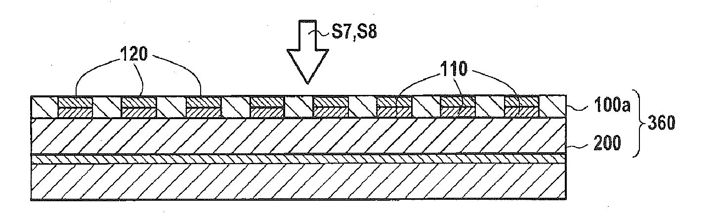
[0045]The invention applies to the direct bonding between two wafers, at least one of these two wafers comprising microcomponents that have been produced before the bonding operation. For the sake of simplification, the term “microcomponents” will refer in the rest of this text to devices or any other features resulting from the technological steps carried out on or in the layers, the positioning of which must be precisely controlled. These may therefore be active or passive components, having simple patterns, contact pads or interconnects.

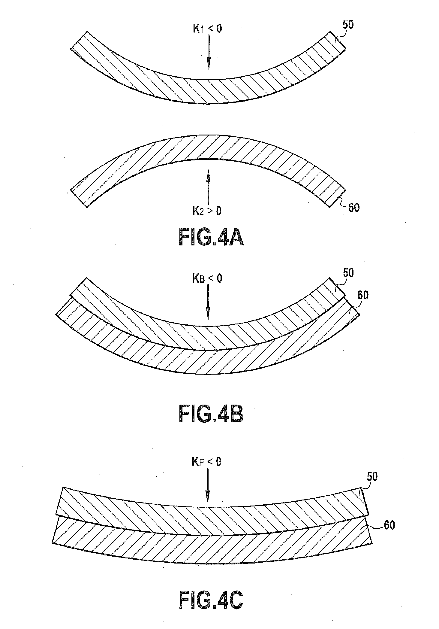
[0046]To reduce the appearance of the overlay effect described above, the present invention proposes to reduce the inhomogeneous deformations of the wafers resulting from being bonded, by imposing on the wafers, during bonding, a bonding curvature that has been defined beforehand depending on the initial curvature of the wafer or wafers comprising the microcomponents.

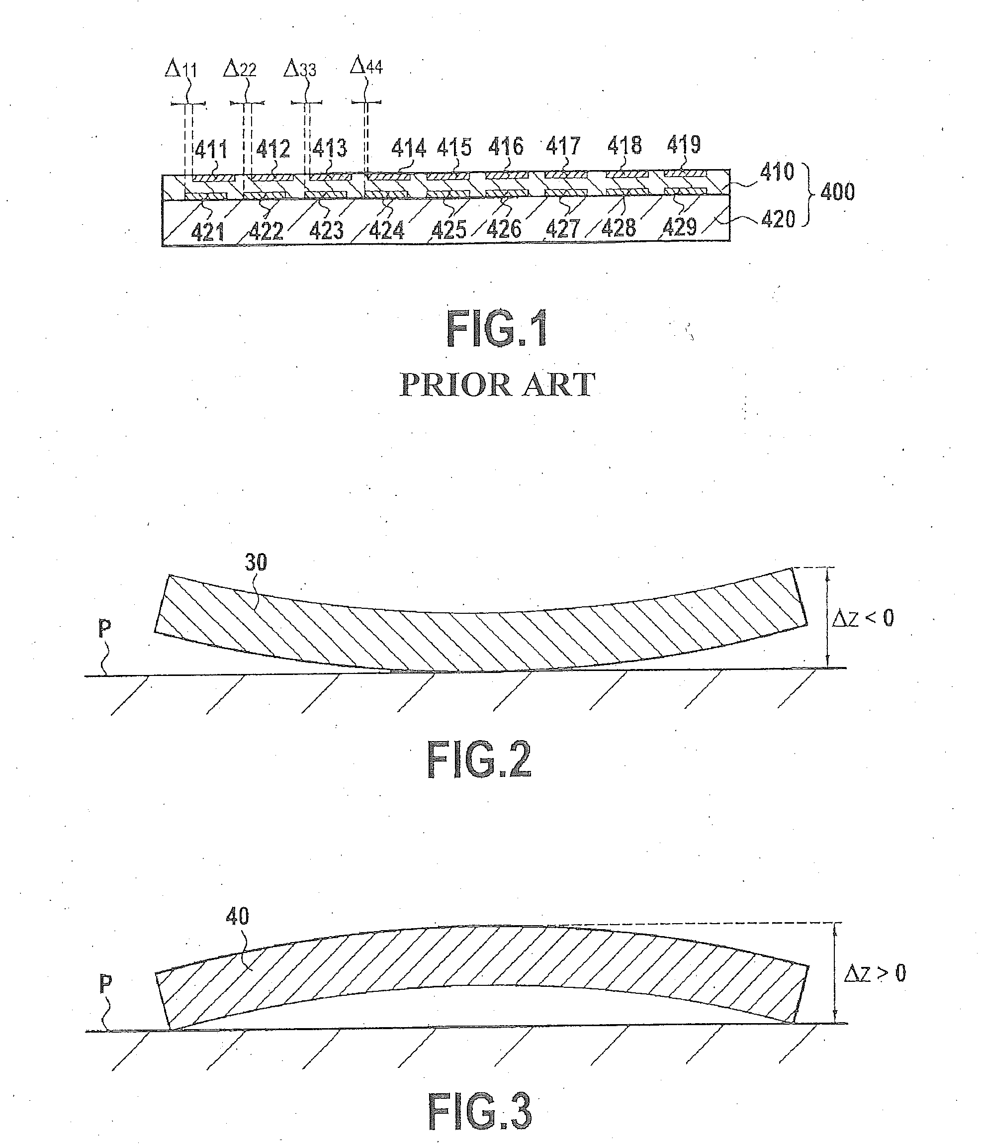
[0047]Before bonding, each wafer has an intrinsic curvature which may be concave,...


PUM

PropertyMeasurementUnit
diameteraaaaaaaaaa
sizeaaaaaaaaaa
intrinsic curvatureaaaaaaaaaa

Abstract

A method for the direct bonding of a first wafer having an intrinsic curvature before bonding to a second wafer having an intrinsic curvature before bonding, at least one of the two wafers comprising at least one series of microcomponents. The method includes of bringing the two wafers into contact with each other so as to initiate the propagation of a bonding wave therebetween while imposing a predefined bonding curvature in the form of a paraboloid of revolution on one of the two wafers depending at least upon the intrinsic curvature before bonding of the wafer that includes the microcomponents, with the other wafer being free to conform to the predefined bonding curvature.

Description

TECHNICAL FIELD AND BACKGROUND ART[0001]The present invention relates to the field of multilayer semiconductor structures or wafers produced according to the three-dimensional (3D) integration technology for transferring, onto a first wafer, called the final substrate, at least one layer formed from a second wafer, this layer corresponding to that portion of the second wafer in which elements, for example a plurality of microcomponents, have been formed, it being possible for the first wafer to be a virgin wafer or to comprise other corresponding elements.[0002]In particular, because of the very small size and the large number of microcomponents present on a given layer, each transferred layer, that is to say each wafer comprising the layer, must be positioned on the final substrate (the first wafer alone or already having other transferred layers) with a correct precision so as to meet an alignment tolerance of around 0.3 microns with the subjacent layer. Furthermore, it may be nec...

Claims


Application Information

Patent Timeline
Patent Type & Authority Applications(United States)
IPC IPC(8): H01L21/30B32B38/18
CPCH01L22/20H01L25/50H01L2224/75702H01L21/187H01L22/12Y10T156/1702H01L2224/80948H01L2224/80357H01L2224/80896H01L2224/94H01L2224/75756H01L24/80H01L2224/80895H01L2224/08146H01L2224/80006H01L24/75H01L24/94H01L2924/00014H01L2224/80H01L21/20
Inventor BROEKAART, MARCELGAUDIN, GWELTAZCASTEX, ARNAUD
Owner S O I TEC SILICON ON INSULATOR THECHNOLOGIES
Why Eureka
Try Eureka