Semiconductor Devices and Methods of Manufacturing Thereof

a technology of semiconductors and semiconductors, applied in the field of semiconductor devices, can solve problems such as loss of yield during fabrication or reduction of product li

Active Publication Date: 2012-04-05
INFINEON TECH AG
View PDF7 Cites 22 Cited by
  • Summary
  • Abstract
  • Description
  • Claims
  • Application Information

AI Technical Summary

Benefits of technology

[0006]These and other problems are generally solved or circumvented, and technical advantages are generally achieved, by illustrative embodiments of the present invention.

Problems solved by technology

However, increasing stress results in many deleterious effects on other processes resulting in yield loss during fabrication or a reduction in product lifetime.

Method used


Image

  • Semiconductor Devices and Methods of Manufacturing Thereof
  • Semiconductor Devices and Methods of Manufacturing Thereof
  • Semiconductor Devices and Methods of Manufacturing Thereof

Examples


Embodiment Construction

[0024]The making and using of various embodiments are discussed in detail below. It should be appreciated, however, that the present invention provides many applicable inventive concepts that can be embodied in a wide variety of specific contexts. The specific embodiments discussed are merely illustrative of specific ways to make and use the invention, and do not limit the scope of the invention.

[0025]In various embodiments, porous layers, such as porous semiconductor layers, are used to relieve stresses both during fabrication and post fabrication thereby improving fabrication yield and product lifetimes.

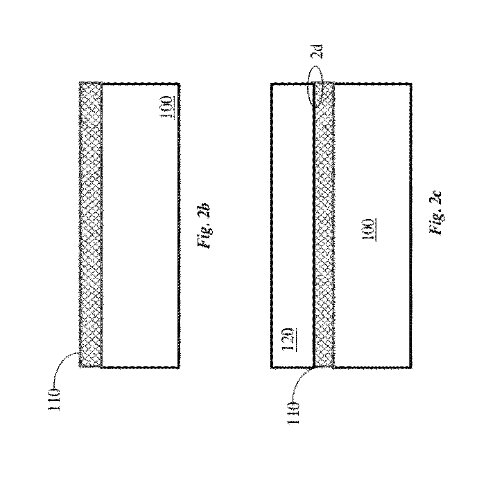
[0026]A structural embodiment of the invention will be described using FIG. 1. Next, methods of fabricating a device using various embodiments of the invention will be described using FIGS. 2-9.

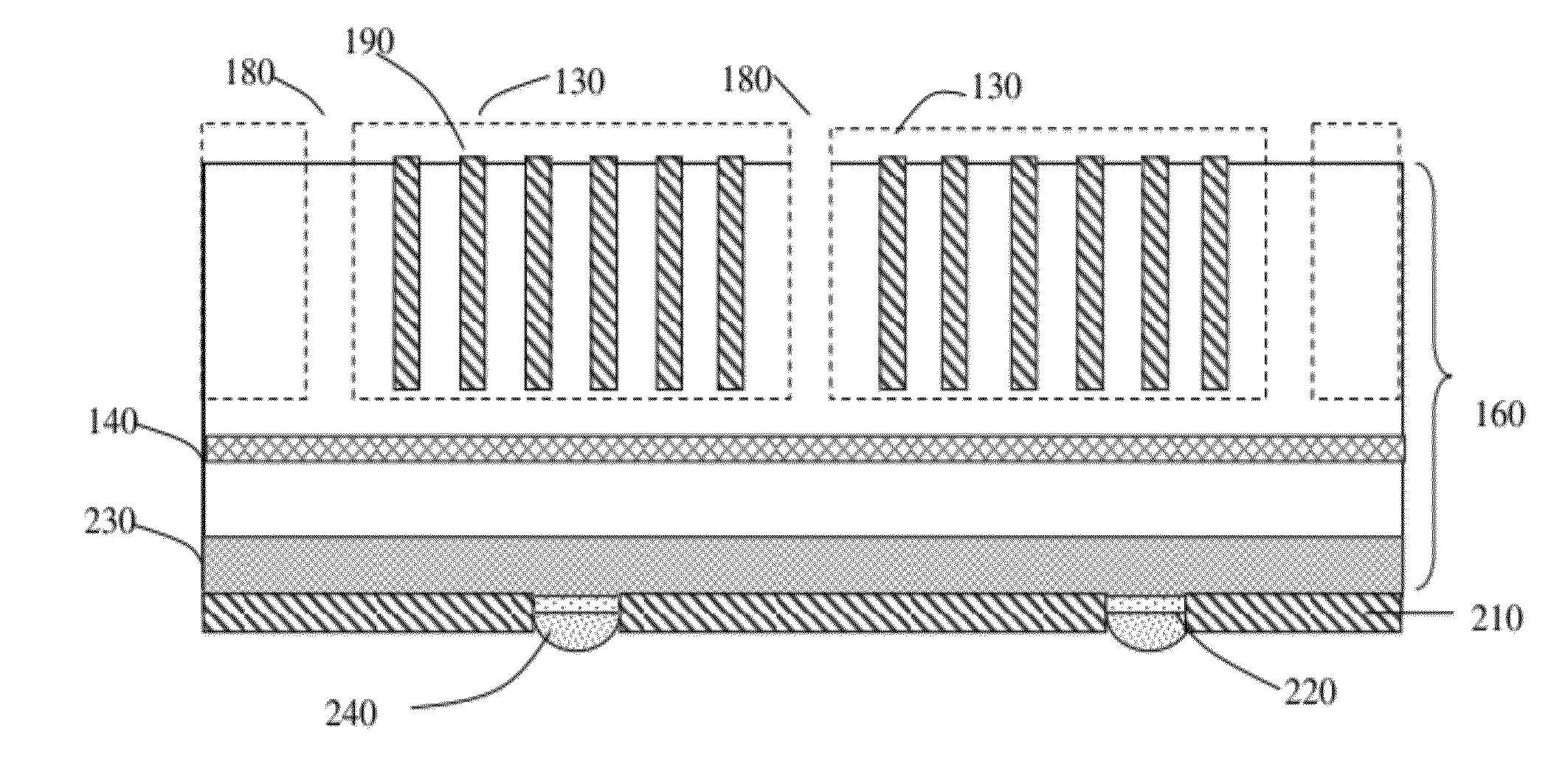
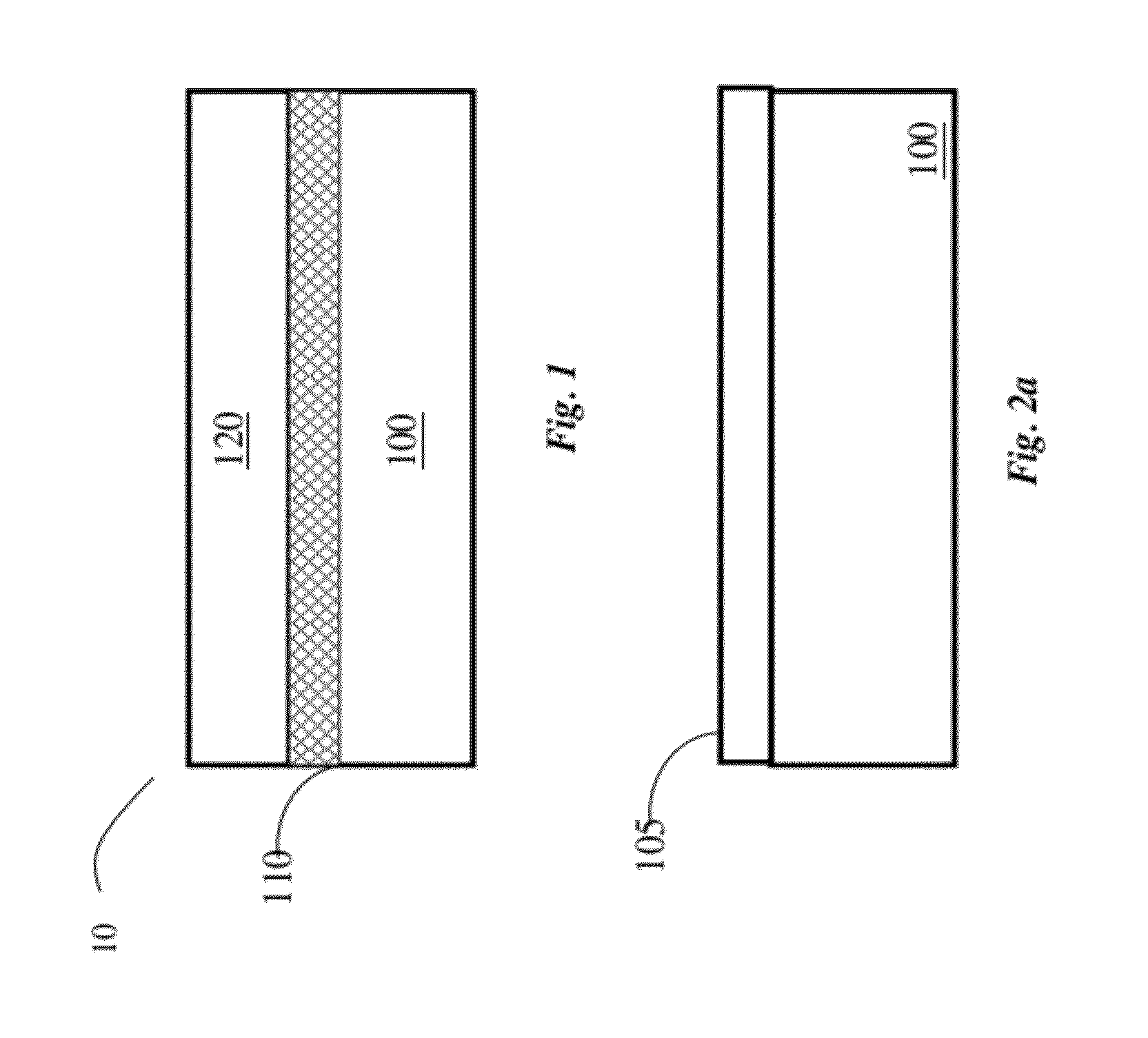
[0027]FIG. 1 illustrates a semiconductor structure in a structural embodiment of the invention. The semiconductor structure 10 may be a portion of a wafer during manufacturing, or in some em...


PUM

PropertyMeasurementUnit
thicknessaaaaaaaaaa
thicknessaaaaaaaaaa
pore sizeaaaaaaaaaa

Abstract

In one embodiment, a method of forming a semiconductor device includes forming a first porous semiconductor layer over a top surface of a substrate. A first epitaxial layer is formed over the first porous semiconductor layer. A circuitry is formed within and over the first epitaxial layer. The circuitry is formed without completely oxidizing the first epitaxial layer.

Description

TECHNICAL FIELD[0001]The present invention relates generally to semiconductors, and more particularly to semiconductor devices and methods of manufacturing thereof.BACKGROUND[0002]Generally, semiconductor devices are used in a variety of electronic applications, such as computers, cellular phones, personal computing devices, and many other applications. Home, industrial, and automotive devices that in the past comprised only mechanical components now have electronic parts that require semiconductor devices, for example.[0003]Semiconductor devices are manufactured by depositing many different types of material layers over a semiconductor workpiece or wafer, and patterning the various material layers using lithography. The material layers typically comprise thin films of conductive, semi-conductive and insulating materials that are patterned and etched to form discrete devices or integrated circuits (ICs). There may be a plurality of transistors, memory devices, switches, conductive l...

Claims


Application Information

Patent Timeline
Patent Type & Authority Applications(United States)
IPC IPC(8): H01L29/20H01L29/04H01L21/20
CPCH01L21/0237H01L21/02381H01L21/0245H01L21/02513H01L21/02521H01L29/7848H01L21/0262H01L21/306H01L21/78H01L29/7846H01L21/02532H01L21/0254H01L21/30621H01L21/3065H01L21/324H01L29/045H01L29/2003H01L29/45
Inventor MAUDER, ANTONSCHULZE, HANS-JOACHIMTIMME, HANS-JOERGHIRLER, FRANZRODRIGUEZ, FRANCISCO JAVIER SANTOS
Owner INFINEON TECH AG
Why Eureka
Try Eureka